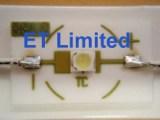
sales5_etlimited_cn china ceramic pcb,china ceramic pcb single layer key speciafications/special features: Base material: Ceramics, Aluminum, Rogers, high Tg, F4B, F4BK, F4BT, TP, PF, FR4, FR1, FR2, CEM-1, CEM-3, etc. pcb Board thickness: 0.30 to
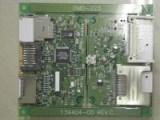
sales+etlimited+cn china pcba supplier,china card read pcba supplier,china 8 layers pcba(pcb assembly) supplier key speciafications/special features: 8 layers PCB Base material: Ceramics, Aluminum, Rogers, high Tg, F4B, F4BK, F4BT, TP, PF, FR4, FR1,
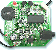
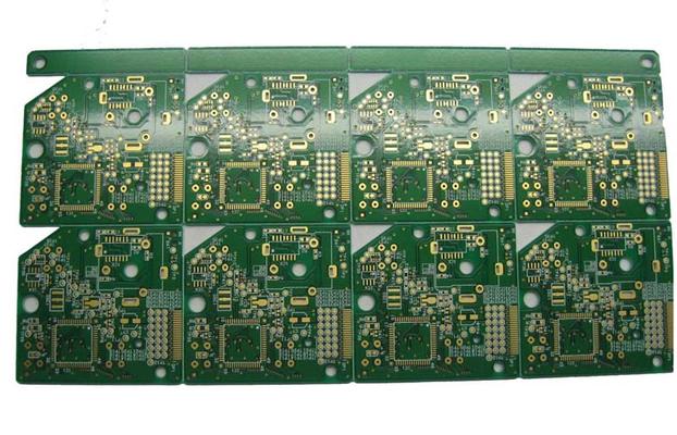
sales5_etlimited_cn Aluminium PCB,single sided PCB,China PCB&PCBA manufacturer key speciafications/special features: 8 layers PCB Base material: Ceramics, Aluminum, Rogers, high Tg, F4B, F4BK, F4BT, TP, PF, FR4, FR1, FR2, CEM-1, CEM-3, etc. Board th
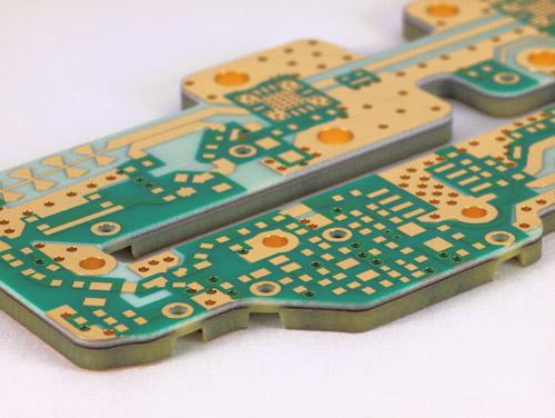
Consisting of multiple laminates and differing dielectric constants, this multilayer (displayed right) is a mixed-dielectric printed circuit board which was manufactured for the Aerospace Industry. Multilayer Mixed Dielectric PCB Specifications:
Industry Directory | Manufacturer
Auspi Enterprises Co., Ltd., one of the professional suppliers of printed circuits in China. We found your company info on the web knowing that you're dealing with electronics, which we think you may have demand on pcbs.
New Equipment | Fabrication Services
Low Cost Heavy Copper PCB China 4 Layers Circuit Boards Supplier Quick Details: FR4 base material 1.6mm board thickness 2oz heavy copper Plating gold finishing RF custom PCB boards Used for Radio Frequency From China PCB manufacturer Specifications
We are electronic contract manufacture and we also have JIT facility. Our head office located in Markham, Ontario, Canada. We do have a facility in USA, MEXICO and BRAZIL.
Industry News | 2017-07-19 21:09:38.0
STI Electronics is pleased to announce the acquisition of a new Fischerscope X-ray XDAL 237 energy dispersive X-ray fluorescence (EDXRF) system.
Technical Library | 2020-08-05 18:49:32.0
The evolution of internet-enabled mobile devices has driven innovation in the manufacturing and design of technology capable of high-frequency electronic signal transfer. Among the primary factors affecting the integrity of high-frequency signals is the surface finish applied on PCB copper pads – a need commonly met through the electroless nickel immersion gold process, ENIG. However, there are well-documented limitations of ENIG due to the presence of nickel, the properties of which result in an overall reduced performance in high-frequency data transfer rate for ENIG-applied electronics, compared to bare copper. An innovation over traditional ENIG is a nickel-less approach involving a special nano-engineered barrier designed to coat copper contacts, finished with an outermost gold layer. In this paper, assemblies involving this nickel-less novel surface finish have been subjected to extended thermal exposure, then intermetallics analyses, contact/sheet resistance comparison after every reflow cycle (up to 6 reflow cycles) to assess the prevention of copper atoms diffusion into gold layer, solder ball pull and shear tests to evaluate the aging and long-term reliability of solder joints, and insertion loss testing to gauge whether this surface finish can be used for high-frequency, high density interconnect (HDI) applications.
Industry News | 2019-11-05 22:19:03.0
> News-Blog > Guideline for wire bonding Guideline for wire bonding Tuesday,Jun 12,2018 There are two wire bonding processes that are used, Thermosonic (T/S) Gold Ball Wire Bonding and Ultrasonic (U/S) Aluminum Wedge Wire Bonding. Approximately 90% of all IC Assembly in Semiconductor Packages is manufactured using Gold Ball Bonding process, while Aluminum Wedge Bonding is used to produce about 10% of other Wire Bonding requirements on Printed Circuit Boards (PCB), Printed Circuit Flex (PCF) and other Packages.


