Parts & Supplies | Assembly Accessories
FUJI IPH4620 DISPERSION SHEET 2,5 FUJI IPH5030 BRACKET FUJI IPH5270 BRUSH FUJI IPH5320 TO IPH-5330 FUJI IPH5330 BRUSH FUJI IPJ1010 GAUGE FUJI IPJ1070 RING FUJI IPJ1090 PIN FUJI IPJ1140 PIN FUJI IPL0410 BELT TIMING FUJI IPL110 Vacuum Pad FU
Used SMT Equipment | In-Circuit Testers
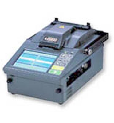
Furukawa S175 Fusion Splicer The Furukawa-Fitel S175 is the fastest, the smallest and the easiest splicer among the world's direct core monitoring machines. It is so easy to use that the splicer automatically analyzes the fibre type from Single
Industry News | 2013-04-27 07:08:56.0
Variety of applications for color sensors - from LED light regulation to the spectral analysis of materials and liquids
New Equipment | Solder Materials
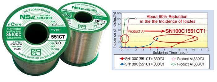
In August 2007, Nihon Superior started simultaneous worldwide sales of SN100C (030) “eCore,” a resin flux cored, lead-free solder product, which contains the newly developed flux that enables the product to display the distinctive features of SN100C
Industry News | 2008-04-22 20:10:56.0
Shimadzu Scientific Instruments: A high-performance, general-purpose instrument, the EDX-720 offers an array of features to deliver enhanced performance and operation, and is an ideal instrument for demanding regulatory compliance measurements such as RoHS and ELV
Used SMT Equipment | General Purpose Test & Measurement
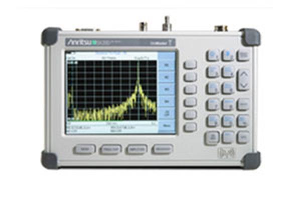
Anritsu Site Master S810D covering 2 MHz to 10.5 GHz is the most accurate, reliable and convenient microwave transmission line and antenna analyzers available for installation, verification, troubleshooting, and repair of microwave communication syst
Technical Library | 2018-04-18 23:55:01.0
Higher functionality, higher performance and higher reliability with smaller real estate are the mantras of any electronic device and the future guarantees more of the same. In order to achieve the requirements of these devices, designs must incorporate fine line and via pitch while maintain good circuitry adhesion at a smooth plating-resin interface to improve signal integrity. The Semi-Additive Process (SAP) is a production-proven method used on low dielectric loss tangent (Df) build-up materials that enables the manufacture of ultra-fine circuitry. (...) This paper will discuss a new SAP process for low loss build-up materials with low desmear roughness (Ra= 40-100 nm) and excellent adhesion (610-680 gf/cm) at various processing conditions. Along with the process flow, the current work will also present results and a discussion regarding characterization on the morphology and composition of resin and/or metal plating surfaces using scanning electron microscopy (SEM) and energy dispersive X-ray spectroscopy (EDX), surface roughness analysis, plating-resin adhesion evaluation from 90o peel tests
Technical Library | 2021-07-13 19:59:34.0
We have investigated the processing of lead-zirconate-titanate-based thick films by inkjet printing Pb (Zr0.53Ti0.47)0.98Nb0.02O3 with a 6 mol% excess of PbO nanosized powder dispersed in water. Differentwaveforms were employed to determine the optimum size and shape of the drops. A uniform, defect-free pattern with dimensions of 4 mm × 4 mm can be printed using 20 V and a drop spacing of 20 μm. The inkjet-printed films were heated to 400 °C to remove the organics and subsequently sintered at 750 and 850 °C. The correlations between the density, grain size and electromechanical properties of the thick films and bulk ceramics are qualitatively discussed. A thickness coupling factor of 46% was obtained for a 15-μm-thick film sintered at low temperature of 850 °C, which is comparable to the value of the bulk ceramic with an identical nominal chemical composition. Our results are important for the economic and environmental-benign printing of piezoelectric materials applicable in variety of electronic devices, such as sensors, actuators, transformers, piezoelectric energy harvesters and transducers.
Technical Library | 2021-10-20 18:21:06.0
The solderability of the SAC305 alloy in contact with printed circuit boards (PCB) having different surface finishes was examined using the wetting balance method. The study was performed at a temperature of 260 _C on three types of PCBs covered with (1) hot air solder leveling (HASL LF), (2) electroless nickel immersion gold (ENIG), and (3) organic surface protectant (OSP), organic finish, all on Cu substrates and two types of fluxes (EF2202 and RF800). The results showed that the PCB substrate surface finish has a strong effect on the value of both the wetting time t0 and the contact angle h. The shortest wetting time was noted for the OSP finish (t0 = 0.6 s with EF2202 flux and t0 = 0.98 s with RF800 flux), while the ENIG finish showed the longest wetting time (t0 = 1.36 s with EF2202 flux and t0 = 1.55 s with RF800 flux). The h values calculated from the wetting balance tests were as follows: the lowest h of 45_ was formed on HASL LF (EF2202 flux), the highest h of 63_ was noted on the OSP finish, while on the ENIG finish, it was 58_ (EF2202 flux). After the solderability tests, the interface characterization of cross-sectional samples was performed by means of scanning electron microscopy coupled with energy dispersive spectroscopy.
Technical Library | 2021-11-03 17:05:39.0
Additively printed circuits provide advantages in reduced waste, rapid prototyping, and versatile flexible substrate choices relative to conventional circuit printing. Copper (Cu) based inks along with intense pulsed light (IPL) sintering can be used in additive circuit printing. However, IPL sintered Cu typically suffer from poor solderability due to high roughness and porosity. To address this, hybrid Cu ink which consists of Cu precursor/nanoparticle was formulated to seed Cu species and fill voids in the sintered structure. Nickel (Ni) electroplating was utilized to further improve surface solderability. Simulations were performed at various electroplating conditions and Cu cathode surface roughness using the multi-physics finite element method. By utilizing a mask during IPL sintering, conductivity was induced in exposed regions; this was utilized to achieve selective Ni-electroplating. Surface morphology and cross section analysis of the electrodes were observed through scanning electron microscopy and a 3D optical profilometer. Energy dispersive X-ray spectroscopy analysis was conducted to investigate changes in surface compositions. ASTM D3359 adhesion testing was performed to examine the adhesion between the electrode and substrate. Solder-electrode shear tests were investigated with a tensile tester to observe the shear strength between solder and electrodes. By utilizing Cu precursors and novel multifaceted approach of IPL sintering, a robust and solderable Ni electroplated conductive Cu printed electrode was achieved.


