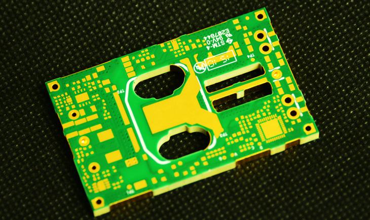
Project Description | Parameters 16 Layer Thickness: 3.8+/-0.03 mm Width/Space: 0.15mm/0.12 mm Surface Treatment: ENIG | Craft Material: SY ST115 Thermal Conductive:1.5W/m.k Back drilling, laser drilling | Application Electronic Power
Industry Directory | Consultant / Service Provider
Laser processing services, laser machining, laser welding, laser drilling , cable assembly, ISO9002
We are a large, Taiwan based, printed circuit board manufacture We specialize in high layer count, HDI process, impedance control and special materials with equipment such as laser drill and horizontal plating
Industrial Laser Cutting, Laser Engraving, Precision Metal Stamping, Precision Drilling, Custom Die Cutting, Rapid Prototypes, Wire Forming, CNC Machining Center in Minnesota
Industry Directory | Manufacturer
Lakeside Sales offers extensive capabilities for PCB's. Quick turn to production. DS to microelectronics ; 4 mil laser drill,
Industry Directory | Consultant / Service Provider
Complete mechanical design and quick-turn machined prototyping services. High vacuum, laser drilling, semi-tools, and handling equipment experience.
Industry Directory | Manufacturer
Pathak machines is a manufacturer involved in the making and supply of highly valued sorts of machine tool like lathe machines, drill machines, milling machines, grinding machines, press machines, CNC.
Technical Library | 2024-04-29 21:39:52.0
In this paper, we develop and put into practice an Automatic Optical Inspection (AOI) system based on machine vision to check the holes on a printed circuit board (PCB). We incorporate the hardware and software. For the hardware part, we combine a PC, the three-axis positioning system, a lighting device and CCD cameras. For the software part, we utilize image registration, image segmentation, drill numbering, drill contrast, and defect displays to achieve this system. Results indicated that an accuracy of 5µm could be achieved in errors of the PCB holes allowing comparisons to be made. This is significant in inspecting the missing, the multi-hole and the incorrect location of the holes. However, previous work only focusses on one or other feature of the holes. Our research is able to assess multiple features: missing holes, incorrectly located holes and excessive holes. Equally, our results could be displayed as a bar chart and target plot. This has not been achieved before. These displays help users analyze the causes of errors and immediately correct the problems. Additionally, this AOI system is valuable for checking a large number of holes and finding out the defective ones on a PCB. Meanwhile, we apply a 0.1mm image resolution which is better than others used in industry. We set a detecting standard based on 2mm diameter of circles to diagnose the quality of the holes within 10 seconds.
With the development of miniaturization of assembly components, the layout area and pattern design area of PCBs have also been continuously reduced, and PCB manufacturers are constantly updating the production process to conform to the development tr
Industry News | 2003-01-28 08:40:56.0
In July 2002, ESI Announced Its Decision to Exit the Mechanical Drilling Business


