Industry Directory | Distributor / Equipment Dealer / Broker / Auctions / Manufacturer
Our company is a global supplier of ready solutions for each process of electronics productions.We supply SMT equipment, PCB cleaning equipment and full range of materials. We make also qualified customer support and spare parts.

New Equipment | Cleaning Equipment
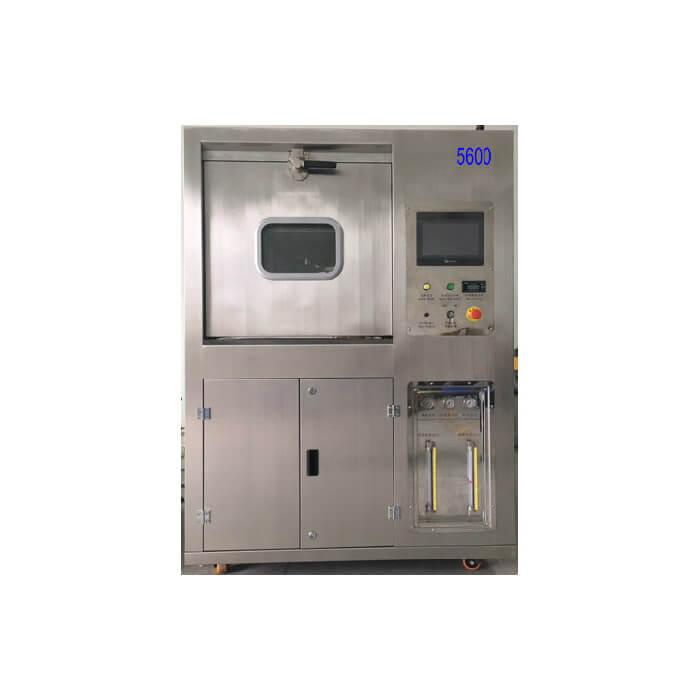
PCBA CLEANING MACHINE 5600 Demensions:600 x 1000 x 1600mm PCB width:50-400mm PCB Length:Max 460mm Pitches:10,20,30mm Product description: PCBA CLEANING MACHINE 5600 INQUIRY PCBA CLEANING MACHINE 5600 Product Introduce:
New Equipment | Cleaning Equipment
SMT Stencil CLEANING MACHINE 5600 Demensions:600 x 1000 x 1600mm PCB width:50-400mm PCB Length:Max 460mm Pitches:10,20,30mm Product description: SMT Stencil CLEANING MACHINE 5600, Demensions:600 x 1000 x 1600mm, PCB width:50-400mm, PCB Length:
Used SMT Equipment | In-Circuit Testers
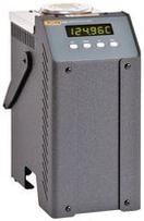
Fluke 6102-156 Micro-Bath Drywell Temperature Calibrator MICRO-BATH, TEMPERATURE, +35*C TO +200*C Micro-Baths can be used anywhere for any type of sensor. The Model 6102 weighs 4.5 kg with the fluid. It's lighter and smaller than most dry-wel
Industry News | 2020-06-24 15:27:46.0
Austin American Technology (AAT) is pleased to offer the Mega ION® cleaning system designed for solvent based, high reliability applications requiring product cleanliness verification (IPC ROSE Testing). It is used for final clean prior to conformal coat, encapsulation or other sealing operations used to protect electronic modules.
Industry News | 2001-06-26 09:54:11.0
The AQS-3500 manual ultrasonic stencil cleaning machine from JNJ Industries, Inc. can accommodate stencils up to 29" x 29". This state of the art system uses integral sweep and pulse ultrasonic generation for optimal cleaning performance. It is equipped with an ergonomically designed control panel that utilizes electromechanical switches and digital timers to control the machine functions.
Technical Library | 2017-04-20 13:51:14.0
The one constant in electronics manufacturing is change. Moore's Law, which successfully predicted a rate of change at which transistor counts doubled on Integrated Circuits (ICs) at lower cost for decades, is ceding to be an appropriate prediction tool. Increasing technical and economic requirements, deriving from the semiconductor environment, are cascaded down to the printed circuit and in particular to the IC substrate manufacturers. This is both a challenge and an opportunity for IC Substrate manufacturers, when dealing with the demands of the packaging market. (...)This paper introduces two new electroless copper baths developed for IC substrates manufacturing based on Semi Additive Process (SAP) technology (hereafter referred to as E'less Copper IC) and HDI production (hereafter referred to as E'less Copper HDI) and optimized for high throw into BMVs. An introduction to reliable throwing power measurement methods based on scanning electron microscope (SEM) is given, followed by a compilation and discussion of key performance criteria for each application, namely throwing power, copper adhesion on the substrate, dry film adhesion and reliability.
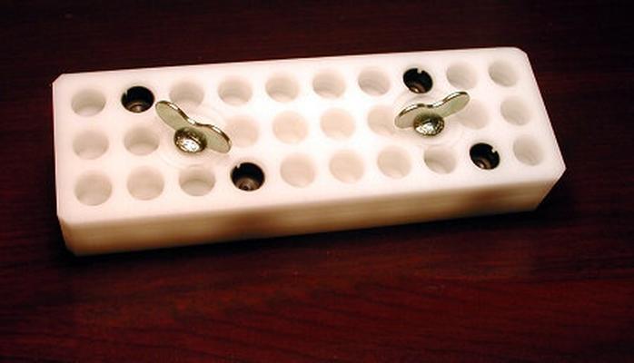
| https://pcbasupplies.com/asm-siemens-siplace-cleaning-fixture/
. By using the 28-Nozzle Cleaning Jig, you can then quickly insert 28 nozzles, then proceed with the ultrasonic bath, rinse, and dry process with the nozzles securely in place
Imagineering, Inc. | https://www.pcbnet.com/blog/what-is-the-pcb-fabrication-process/
. The plate is then removed and placed into a tin plating bath to serve as an etch barrier. As plating is completed, the dry film is removed and the exposed copper not cover by tin is etched away, leaving only the traces, pads, and other patterns on the plate