Events Calendar | Wed Dec 04 00:00:00 EST 2019 - Fri Dec 06 00:00:00 EST 2019 | Shenzhen, China
2019 International Electronics Circuit Exhibition
Industry News | 2006-02-07 02:17:46.0
Press Release
Industry News | 2006-02-01 09:05:56.0
Discover the Solderite Difference
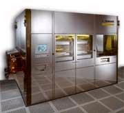
SUSS MicroTec's newest product offering is a 300 mm lithography cluster which consists of an MA300 mask aligner module linked to an ACS300 spin-coating system. LithoPack300 (LP300) is specifically designed for wafer bumping and wafer level packaging
New Equipment | Test Equipment
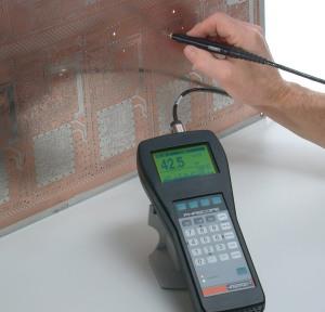
The hand-held PHASCOPE® PMP10 is ideally suited for quality control in the electroplating and printed circuit board (PCB) industries. Because the instrument employs the phase-sensitive eddy current method (ISO 21 968), it allows the measurement of me

In-House PCB Through-Hole Plating without Chemicals The LPKF ProConduct® introduces revolutionary technology to produce plated through-holes, which does not require a plating tank or potentially hazardous processing chemicals. This compact system is
Technical Library | 2019-07-17 17:56:34.0
The increased demand for electronic devices in recent years has led to an extensive research in the field to meet the requirements of the industry. Electrolytic copper has been an important technology in the fabrication of PCBs and semiconductors. Aqueous sulfuric acid baths are explored for filling or building up with copper structures like blind micro vias (BMV), trenches, through holes (TH), and pillar bumps. As circuit miniaturization continues, developing a process that simultaneously fills vias and plates TH with various sizes and aspect ratios, while minimizing the surface copper thickness is critical. Filling BMV and plating TH at the same time, presents great difficulties for the PCB manufactures. The conventional copper plating processes that provide good via fill and leveling of the deposit tend to worsen the throwing power (TP) of the electroplating bath. TP is defined as the ratio of the deposit copper thickness in the center of the through hole to its thickness at the surface. In this paper an optimization of recently developed innovative, one step acid copper plating technology for filling vias with a minimal surface thickness and plating through holes is presented.
Industry News | 2019-05-16 01:24:13.0
With the development of miniaturization of assembly components, the layout area and pattern design area of PCBs have also been continuously reduced, and PCB manufacturers are constantly updating the production process to conform to the development trend. The application of the resin plugging process has also become more and more extensive, and it has been used in HDI panels.
Industry News | 2020-10-04 15:41:30.0
MacDermid Alpha Electronics Solutions will be exhibiting at the Taiwan Printed Circuit Association (TPCA) exhibition and presenting two technical papers at the IMPACT-EMAP Conference, co-located with TPCA in Taipei, October 21-23, 2020. The papers detail some of the ways in which MacDermid Alpha has invested in the research of innovative manufacturing processes to meet the demanding standards required for the new age of miniaturization.
Industry News | 2021-12-17 16:40:06.0
MacDermid Alpha Electronics Solutions will exhibit its total process solutions for the emerging semiconductor market at the Semicon Taiwan, Taipei City, December 28-30, 2021 at Taipei Nangang Exhibition Center, Hall 1 (TaiNEX 1).


