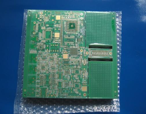
Bicheng provides impedance controlled PCB's for R&D, high-tech, IT research companies and organizations, large or small. Technical parameters *Controlled dielectric *Controlled impedance *Design coupons *Test coupons *Po
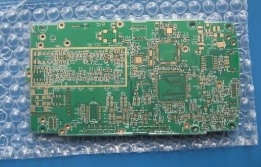
600V *RO4350B *RO4003C Dielectric material & Stack up requirement FR-4(no copper): 0.05-3.2mm for option Prepreg type: 7628H(7630), 7628(43%), 7628(41%), 2116HR, 2116, 2113, 1080 and 1060 for option Copper
Electronics Forum | Fri Jul 23 10:08:31 EDT 2004 | B. Hunter
We received bare PCB's that were supposed to have been finished with immersion silver because of BGA locations. The boards were finished in ENIG. We are concerned over any reliabilty problems that might occur as a result of using ENIG at BGA locati
Electronics Forum | Wed Apr 06 13:43:14 EDT 2011 | mosborne1
ENIG is the way you need to go. With ENIG you deposit a lot less gold. Too much gold will cause soler problems. Matt www.americancircuits.com
Industry News | 2004-02-04 16:52:03.0
Prepare for the 2006 European Deadline
Industry News | 2012-01-17 11:05:35.0
Practical Components introduces a test board for its dummy (mechanical sample) version of Amkor’s cutting-edge 0.3 mm pitch CVBGA. Amkor’s new semiconductor device is a wafer-scale package in a miniature package, which is suitable for installation in surface mount technology (SMT). Amkor’s ChipArray® range of packages consists of laminate-based ball grid array (BGA) packages that are compatible with established SMT mounting processes.
Technical Library | 2019-06-07 14:49:54.0
ACI Technologies was contacted in regards to poor solder joint reliability. The customer submitted an assembly that was exhibiting intermittent opens at multiple locations on a ball grid array (BGA) component. The assembly’s functionality did not survive international shipping, essentially shock and vibration failures, immediately making the quality of the solder joints suspect. The customer was asked about the contract manufacturer and the reflow oven profile as well as the solder paste and surface finish used. The ACI engineering staff evaluated the contract manufacturer’s technique and determined that they were competent in the methods they used for placing thermocouples in the proper locations and developing the reflow oven profile. The surface finish was unusual, but not unheard of, in that it was hard gold over hard nickel, rather than electroless nickel immersion gold (ENIG). The customer was able to supply boundary scan testing data which showed a diagonal row of troublesome BGA pins.
Technical Library | 2008-04-08 17:42:27.0
Concern about the failure of lead-free BGA packages when portable devices such as cell phones are accidentally dropped and a general concern about the resistance of these packages under shock loading has prompted an interest in the impact strength of the soldered BGA connection. This paper reports the results of the measurement of the impact strength of lead-free 0.5±0.01mm diameter BGA spheres on 0.42mm solder mask defined pads on copper/OSP and ENIG substrates using recently developed equipment that can load individual BGA spheres at high strain rates in shear and tension.
Career Center | Phoenix, Arizona | Engineering,Management,Production,Quality Control,Research and Development,Sales/Marketing,Technical Support
• Highly motivated, solution oriented professional with proven record synergizing scientific, engineering, and business administration backgrounds to drive and sustain customer satisfaction and long term improvements. • Articulate communicator that a
SMTnet Express, January 23, 2014, Subscribers: 26486, Members: Companies: 13559, Users: 35667 Testing Intermetallic Fragility on Enig upon Addition of Limitless Cu by Martin K. Anselm, Ph.D. and Brian Roggeman; Universal Instruments Corp
Imagineering, Inc. | https://www.pcbnet.com/capabilities/assembly/technology-roadmap/
. Layer Count 50 Max. Working Panel Size 21" x 31" Max. Board Thickness .300" Min. Board Thickness 0.16"(6L) Min. Line/Space • I/L - 2 / 1.5mil (HDI) • O/L - 2 / 1.5 mil (HDI) Warpage .001" / sq. in. BGA Pitch 0.20mm Layer to Layer Registration 3 mil


