New Equipment | Fabrication Services
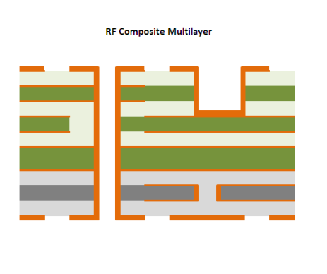
Multilayer PCB's ACI manufactures a wide variety of Multilayer PCB's for various applications spanning numerous industries and technologies. We can build your high layer count PCB's using a wide variety of high speed low loss materials from epoxies
New Equipment | Assembly Services
The board is designed by customer and it's for Set-Top Box PCBA board. We did one-Stop EMS Service for this project (PCB manufacture, components sourcing, SMT and THT assembly): Product name: 4 Layer PCBA board Material: FR-4 TG180, Shengyi Thicknss
New Equipment | Assembly Services
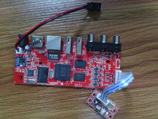
The board is designed by customer and it's for TV Box PCBA board. We did One-Stop EMS Service for this project (PCB manufacture, components sourcing, SMT and THT assembly). Product name: 4 Layer PCBA board Material: FR-4 TG170 Thicknss: 1.6mm Surfac
New Equipment | Assembly Services
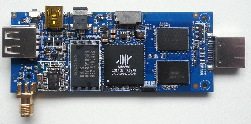
The board is designed by customer and it's for Network interface controller. We did one-Stop EMS Service for this project (PCB manufacture, components sourcing, SMT and THT assembly): Product name: 8 Layer HDI PCBA board Material: FR-4 TG180, Shengy
Industry News | 2019-11-05 22:19:03.0
> News-Blog > Guideline for wire bonding Guideline for wire bonding Tuesday,Jun 12,2018 There are two wire bonding processes that are used, Thermosonic (T/S) Gold Ball Wire Bonding and Ultrasonic (U/S) Aluminum Wedge Wire Bonding. Approximately 90% of all IC Assembly in Semiconductor Packages is manufactured using Gold Ball Bonding process, while Aluminum Wedge Bonding is used to produce about 10% of other Wire Bonding requirements on Printed Circuit Boards (PCB), Printed Circuit Flex (PCF) and other Packages.
Industry News | 2010-04-10 23:59:50.0
LOS ALAMITOS, CA - Following the success of their 2007 test board and kit, Practical Components and Aim Solder have updated their offering with a new AIM print test board and kit that is designed to include many printing challenges commonly found in manufacturers' assemblies.
Industry News | 2019-11-05 22:07:01.0
Tenting a via refers to covering via with soldermask to enclose or skin over the opening. A via is a hole drilled into the PCB that allows multiple layers on the PCB to be connected to each other. A non tented via is just a via that is not covered with the soldermask layer. Leaving these vias exposed or covered has pros and cons depending on the your design and manufacturing requirements.
Electronics Forum | Mon Aug 16 11:49:44 EDT 2004 | Kris
Hi Guys thanks for the replies. Dave, the spec is not for enig but for hard gold does your response alter if thats the case /
Electronics Forum | Mon Aug 16 16:37:08 EDT 2004 | davef
As we mentioned in an earlier response in this thread [Q5], you do NOT want to solder to hard gold. Hard gold is a wear surface. [That's IT, that's the LIST.] If you want to solder to gold, then either use: * IPC-4552 ENIG specification, mentioned
Electronics Forum | Mon Aug 16 13:18:46 EDT 2004 | davef
You bet our reponse changes. Q2R: Hard gold thickness is 4 to 10 u" for Au and 300 to 400 u" for nickel A2R: This is a hard gold spec?? It looks like a ENIG spec. Although, the Ni is quite heavy, 150 uin is sufficient for most applications. The gol


