Industry Directory | Manufacturer
Shenzhen Beyond Laser Technology Co., LTD specialize in laser equipment since 2009, the world leading precision laser machine manufacturer
Corporation Japanese etched circuit manufacturer's association (Japan Electronics Packaging and Circuits Association: JPCA)
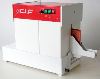
Double sided model with rinsing and thermostated heater. Etching time 2 minutes with a new ferric chloride at 30°C. Integrated heater Strong Performent Economic & speed Recommended for SMT cards Welded PVC
A six person Rep. Agency serving the S.E. USA since 1986. We assist our customers with design services in industrial, telecommunications, medical, automotive and appliance manufacturers. Products and Services: Electrical; pcb's, connectors, wire,
Electronics Forum | Thu Jun 03 12:41:49 EDT 2021 | k_moore
Hello people. We have a Nutek LMC-S3 laser etcher that we use for etching 2D datamatrix codes onto our PCBs. The system has been in use for some time, but seems to constantly need tweaking to get reliable results. There are a lot of variables that
Electronics Forum | Thu Jun 03 17:29:21 EDT 2021 | emeto
From what I figured, machine is as good as the understanding we have about it. I have heard people complaining about machines I know for a fact are great. Manuals and training are there with a reason. There is no universal recipe for anything out the
Used SMT Equipment | General Purpose Equipment
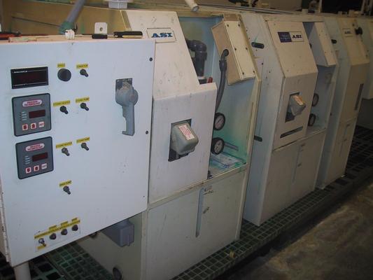
ASI Etcher 2' Etch Spray Chamber 2' Etch Spray Chamber 1' Recirc. Rinse 1' Cascade spray Dimensions: 10.5' Long x 5' Wide 480V 40A 3Ph All rewired with contactors,heatercontrollers,ect. Full Schematic of Machine Shipping- This item will be on oversi
Industry News | 2003-03-21 08:12:24.0
Tecan reckons it is consistently producing what may be regarded as the most efficient stencils in the world today.
Industry News | 2014-07-21 13:55:54.0
Briefing Co-hosted by IPC as Part of Continuing Effort to Connect IPC Members with Policymakers
Parts & Supplies | Pick and Place/Feeders
SMT spare parts on stock If you interested, just contact us!!! Email: wendy@leadersmt.com Whatsapp: +86 13148795469
Technical Library | 2013-08-08 15:23:11.0
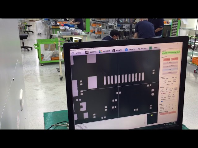
In this project Machine Vision PCB Inspection System is applied at the first step of manufacturing, i.e., the making of bare PCB. We first compare a PCB standard image with a PCB image, using a simple subtraction algorithm that can highlight the main problem-regions. We have also seen the effect of noise in a PCB image that at what level this method is suitable to detect the faulty image. Our focus is to detect defects on printed circuit boards & to see the effect of noise. Typical defects that can be detected are over etchings (opens), under-etchings (shorts), holes etc...
Technical Library | 2020-03-26 14:55:29.0
This paper introduces line confocal technology that was recently developed to characterize 3D features of various surface and material types at sub-micron resolution. It enables automatic microtopographic 3D imaging of challenging objects that are difficult or impossible to scan with traditional methods, such as machine vision or laser triangulation.Examples of well-suited applications for line confocal technology include glossy, mirror-like, transparent and multi-layered surfaces made of metals (connector pins, conductor traces, solder bumps etc.), polymers (adhesives, enclosures, coatings, etc.), ceramics (components, substrates, etc.) and glass (display panels, etc.). Line confocal sensors operate at high speed and can be used to scan fast-moving surfaces in real-time as well as stationary product samples in the laboratory. The operational principle of the line confocal method and its strengths and limitations are discussed.Three metrology applications for the technology in electronics product manufacturing are examined: 1. 3D imaging of etched PCBs for micro-etched copper surface roughness and cross-sectional profile and width of etched traces/pads. 2. Thickness, width and surface roughness measurement of conductive ink features and substrates in printed electronics applications. 3. 3D imaging of adhesive dots and lines for shape, dimensions and volume in PCB and product assembly applications.
World's leading solder paste stencil & emulsion screen inspection system. Used by both stencil/screen fabricators and users to detect errors BEFORE production, eliminating costly rework, scrap and delays. Supports E-form, laser cut, chem etch, hybrid
LSMO-105 fastest and most reliable stencil inspection machine www.aoivision.com
Career Center | Racine, Wisconsin USA | Engineering,Maintenance,Production,Technical Support
We are currently seeking a SMT Process Technician to join our already strong team in a state-of-the-art SMT/PTH facility, only 5 years old. This position will be responsible for all aspects of printed circuit board assembly, from programming of eq
Career Center | Racine, Wisconsin USA | Engineering,Maintenance,Technical Support
SMT Technician Cree Lighting a Company of Ideal Industries (located in Racine, WI and Durham, NC) is a market-leading innovator of Indoor, Outdoor, and Consumer Bulb LED lighting. We are uniquely positioned to innovate new ways in which light
Career Center | Shen Zhen, China | Management,Sales/Marketing
Working in GLORYPCB for 10 years.knowing electronic supply chain very well. especially for PCB PCBA assembly and other Electronic Manufacturing Service.Glorypcb is a professional electronic manufacturer located in Shenzhen with three facilities.offe
Career Center | , | Engineering,Production
Project Management, SMT Process Engineering
ASYMTEK Products | Nordson Electronics Solutions | https://www.nordson.com/en/our-company/news-room/feature-content-roll-up-page/adhesive-dispensing-systems-adds-vision-based-inspection-system-to-improve-quality-and-efficiency
. This is a significant upgrade from the old optical comparator, which would bottleneck work while being done in-process. Together with the Chiron machining centers added to the facility in 2014 and a new laser etching machine for identification marking, the Keyence vision-based inspection machine is helping improve
PCB Libraries, Inc. | https://www.pcblibraries.com/forum/topic1733&OB=DESC.html
. The pcb manufacturer applies a correction factor to the pcb due to the etching. Creating a footprint with a fabrication tolerance is to apply twice this tolerance


