Industry News | 2014-03-04 11:29:02.0
Indium Corporation will feature its new high-melting lead-free solder paste technology, BiAgX™, at Semicon China on March 18-20 in Shanghai, China.
Industry News | 2014-01-31 00:23:23.0
Indium Corporation announces a new solder paste technology. BiAgX™ is a high-melting lead-free (Pb-free) solder paste technology designed for high reliability electronics assembly applications. Designed as a drop-in replacement for standard high Pb-containing solder pastes, it has passed MSL1 and thermal cycle testing at several power semiconductor customers.
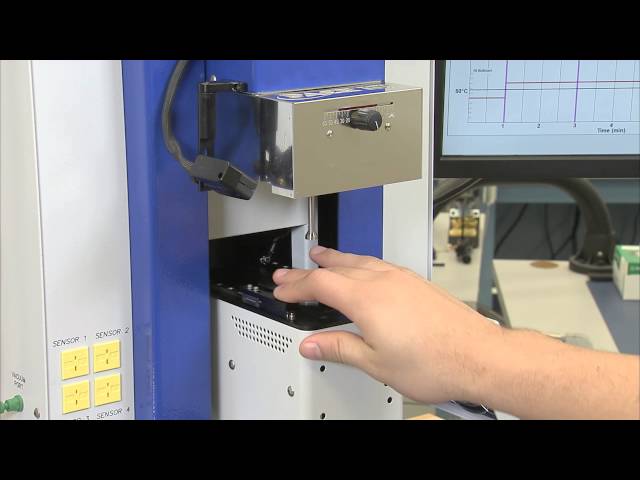
"The IR 3000 offers advanced surface mount rework capability in an integrated, cost-effective, bench-top work station." This video covers the basic processes of the IR 3000, focusing primarily on: Installations, Removals, Component Alignment and Ins
New Equipment | Rework & Repair Equipment
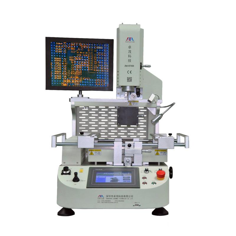
SMT solution provider with X-ray inspection machine, X-ray components counter and BGA repairing machine Contact me for more information: Skype:ritaleeli Email:sales11@zhuomao.com.cn Whatsapp/wechat: 0086 134 3448 1030 Semi-auto BGA Rework St
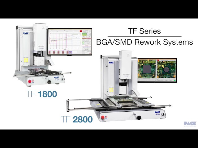
Enter PACE’s TF Series BGA/SMD Rework Systems. With its groundbreaking, patented Inductive-Convection Heating Technology, the TF Series top-side heater reaches the target temperature in just seconds for safe, rapid solder joint reflow in virtually an
Enter PACE’s TF Series BGA/SMD Rework Systems. With its groundbreaking, patented Inductive-Convection Heating Technology, the TF Series top-side heater reaches the target temperature in just seconds for safe, rapid solder joint reflow in virtually an
Industry News | 2013-04-03 18:52:22.0
SMART Group,announces that on 26th March 2013, more than 30 delegates from manufacturing and service repair sectors, including line managers, process and quality engineers, attended its successful “Back to Basics” Hands-on Rework and Inspection Workshop at the Manufacturing Technology Centre in Coventry, UK
Industry News | 2014-08-14 21:44:44.0
Several Indium Corporation experts will share their technical knowledge with attendees at the Surface Mount Technology Association's International Conference and Exhibition (SMTAi) from Sept. 28-Oct. 2 in Rosemont, Ill.
Industry News | 2019-11-05 22:08:21.0
Via in pad is the design practice of placing a via in the copper landing pad of a component. Compared to standard PCB via routing, via in pad allows a design to use smaller component pitch sizes and further reduce the PCBs overall size. With component manufactures pushing smaller parts every year and the demand from consumers for smaller devices, the usage of via in pad practices by hardware engineers have become more commonplace. In this article, we will discuss the differences between via in pad and traditional vias, when should you use via in pad, and how to design for it.
Electronics Forum | Wed Jul 08 15:18:20 EDT 1998 | Upinder Singh
We are wave soldering a board having 24 similar thru hole connectors on it, using a wave soldering pallet. The problem is that one particular pin of connector in around 6-9 connectors get excess solder on the bottom side. I have tried all the parame

COT specializes in high quality SMT nozzles and consumables for pick and place machines. We provide special engineering design service of custom nozzles for those unique and odd components.
2481 Hilton Drive
Gainesville, GA USA
Phone: (770) 538-0411


.png)
