Technical Library | 2020-09-02 22:02:13.0
With the adoption of Wafer Level Packages (WLP) in the latest generation mobile handsets, the Printed Circuit Board (PCB) industry has also seen the initial steps of High Density Interconnect (HDI) products migrating away from the current subtractive processes towards a more technically adept technique, based on an advanced modified Semi Additive Process (amSAP). This pattern plate process enables line and space features in the region of 20um to be produced, in combination with fully filled, laser formed microvias. However, in order to achieve these process demands, a step change in the performance of the chemical processes used for metallization of the microvia is essential. In the electroless Copper process, the critical activator step often risks cross contamination by the preceding chemistries. Such events can lead to uncontrolled buildup of Palladium rich residues on the panel surface, which can subsequently inhibit etching and lead to short circuits between the final traces. In addition, with more demands being placed on the microvia, the need for a high uniformity Copper layer has become paramount, unfortunately, as microvia shape is often far from ideal, the deposition or "throw" characteristics of the Copper bath itself are also of critical importance. This "high throwing power" is influential elsewhere in the amSAP technique, as it leads to a thinner surface Copper layer, which aids the etching process and enables the ultra-fine features being demanded by today's high end PCB applications. This paper discusses the performance of an electroless Copper plating process that has been developed to satisfy the needs of challenging amSAP applications. Through the use of a radical predip chemistry, the formation, build up and deposition of uncontrolled Pd residues arising from activator contamination has been virtually eradicated. With the adoption of a high throwing power Copper bath, sub 30um features are enabled and microvia coverage is shown to be greatly improved, even in complex via shapes which would otherwise suffer from uneven coverage and risk premature failure in service. Through a mixture of development and production data, this paper aims to highlight the benefits and robust performance of the new electroless Copper process for amSAP applications
Printed circuit boards lacked with a green solder mask are - including SMT components - essential for soldering safely. Learn more: http://www.lpkf.com/products/rapid-pcb-prototyping/solder-masks-legend-printing/index.htm?utm_source=youtube&utm_mediu
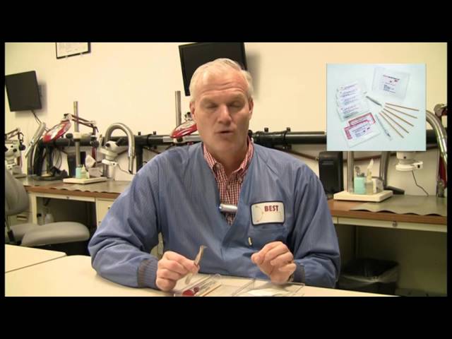
The BEST PCB pad repair repair kit gives you the tools you need for fast modification and repair of PCB circuit pads-no matter what their size. Our online PCB repair training videos, our master instructors along with these materials allows you to mee

In the world of makers, people enjoy the fun of designing and developing hardware/ software, even final electronic products. They will not concentrate a lot on the cost and manufacturability. But it is quite different from lab to factory, when it com
Technical Library | 2015-12-02 18:32:50.0
(Thermal Compression with Non-Conductive Paste Underfill) Method.The companies writing this paper have jointly developed Copper (Cu) Pillar micro-bump and TCNCP(Thermal Compression with Non-Conductive Paste) technology over the last two+ years. The Cu Pillar micro-bump and TCNCP is one of the platform technologies, which is essentially required for 2.5D/3D chip stacking as well as cost effective SFF (small form factor) package enablement.Although the baseline packaging process methodology for a normal pad pitch (i.e. inline 50μm) within smaller chip size (i.e. 100 mm2) has been established and are in use for HVM production, there are several challenges to be addressed for further development for commercialization of finer bump pitch with larger die (i.e. ≤50μm tri-tier bond pad with the die larger than 400mm2).This paper will address the key challenges of each field, such as the Cu trace design on a substrate for robust micro-joint reliability, TCNCP technology, and substrate technology (i.e. structure, surface finish). Technical recommendations based on the lessons learned from a series of process experimentation will be provided, as well. Finally, this technology has been used for the successful launching of the company FPGA products with SFF packaging technology.
Left: This part looked ok to the naked eye. Right: A microscopic view shows evidence of this part being previously soldered or reworked. Another part caught and prevented from being a potential problem for our customer. Decapsulation, Pinpri
New Equipment | Solder Materials
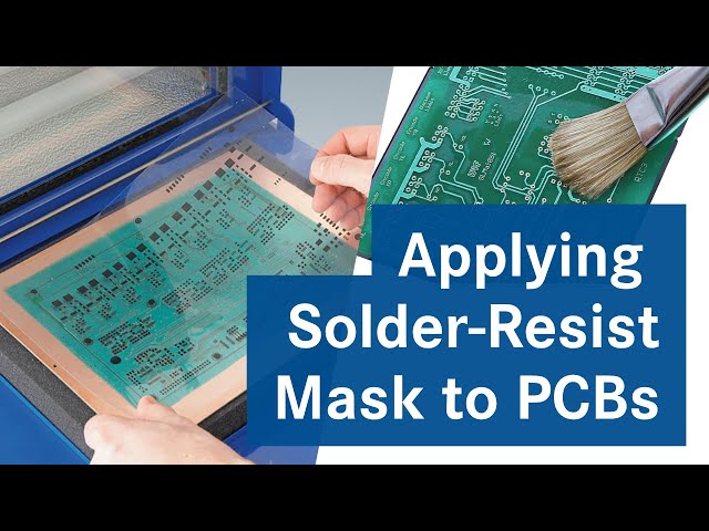
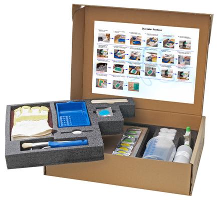
An easy-to-use cost-effective solution for producing professionally masked PCBs in an in-house prototyping environment. Compact, quick and easy to use Professional finish and perfect soldering Four simple steps to a professional result
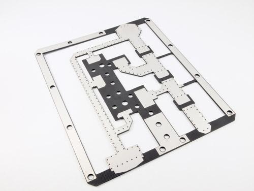
With a combination of specialized processes and equipment, the boards were custom manufactured from double-sided glass-reinforced PTFE. This PCB is used for controlled impedance within a microwave application.. Utilizing advanced photolithography a

Molex's membrane switches provide durable, lightweight and low-profile options for integrating user interfaces and electronic components into a variety of applications including medical, industrial and commercial products. Molex standard membrane s
Industry News | 2018-10-18 08:29:16.0
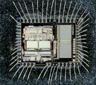
How to Prevent Short Circuits to Ground in QFN Components?


