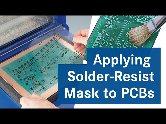
Printed circuit boards lacked with a green solder mask are - including SMT components - essential for soldering safely. Learn more: http://www.lpkf.com/products/rapid-pcb-prototyping/solder-masks-legend-printing/index.htm?utm_source=youtube&utm_mediu
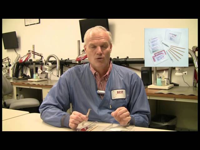
The BEST PCB pad repair repair kit gives you the tools you need for fast modification and repair of PCB circuit pads-no matter what their size. Our online PCB repair training videos, our master instructors along with these materials allows you to mee
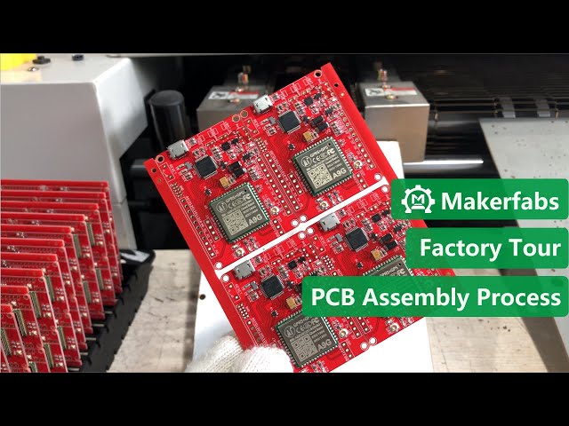
In the world of makers, people enjoy the fun of designing and developing hardware/ software, even final electronic products. They will not concentrate a lot on the cost and manufacturability. But it is quite different from lab to factory, when it com
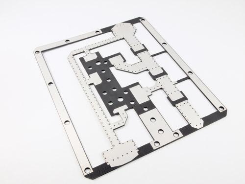
With a combination of specialized processes and equipment, the boards were custom manufactured from double-sided glass-reinforced PTFE. This PCB is used for controlled impedance within a microwave application.. Utilizing advanced photolithography a
Technical Library | 2021-11-03 17:05:39.0
Additively printed circuits provide advantages in reduced waste, rapid prototyping, and versatile flexible substrate choices relative to conventional circuit printing. Copper (Cu) based inks along with intense pulsed light (IPL) sintering can be used in additive circuit printing. However, IPL sintered Cu typically suffer from poor solderability due to high roughness and porosity. To address this, hybrid Cu ink which consists of Cu precursor/nanoparticle was formulated to seed Cu species and fill voids in the sintered structure. Nickel (Ni) electroplating was utilized to further improve surface solderability. Simulations were performed at various electroplating conditions and Cu cathode surface roughness using the multi-physics finite element method. By utilizing a mask during IPL sintering, conductivity was induced in exposed regions; this was utilized to achieve selective Ni-electroplating. Surface morphology and cross section analysis of the electrodes were observed through scanning electron microscopy and a 3D optical profilometer. Energy dispersive X-ray spectroscopy analysis was conducted to investigate changes in surface compositions. ASTM D3359 adhesion testing was performed to examine the adhesion between the electrode and substrate. Solder-electrode shear tests were investigated with a tensile tester to observe the shear strength between solder and electrodes. By utilizing Cu precursors and novel multifaceted approach of IPL sintering, a robust and solderable Ni electroplated conductive Cu printed electrode was achieved.
Industry News | 2019-11-05 22:26:14.0
The board stack-up is probably the most essential piece for ensuring a successful PCB design. Modern high-speed boards require controlled-impedance traces, and whether you are using a simulation tool, a simple calculator, or the back of a napkin, you need to understand your manufacturing process to correlate your impedance calculations. This ensures that your trace widths and dielectric heights match what will actually be manufactured, and eliminates last-minute design changes.
Industry Directory | Consultant / Service Provider / Manufacturer
Tropical Stencil is dedicated to providing the highest quality Laser Cut Stencils; with our rapid response, you will have your Stencil delivered on-time.
Industry Directory | Manufacturer
Military Certified PCB Fabrication & Circuit Board Assembly Manufacturer Custom PCB fabrication in as little as 8 hours – All you have to do is ask! 16 Years Of PCB Manufacturing - Serving Electronic Since 2001
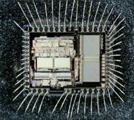
Left: This part looked ok to the naked eye. Right: A microscopic view shows evidence of this part being previously soldered or reworked. Another part caught and prevented from being a potential problem for our customer. Decapsulation, Pinpri
New Equipment | Solder Materials
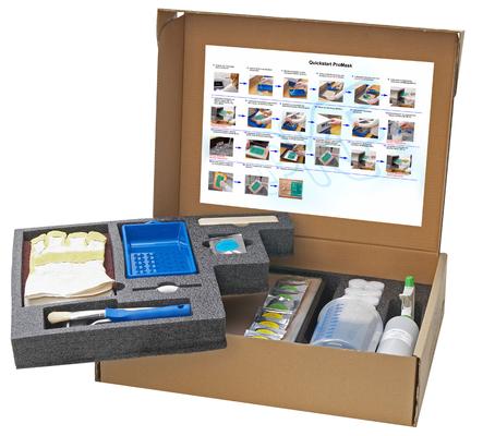
An easy-to-use cost-effective solution for producing professionally masked PCBs in an in-house prototyping environment. Compact, quick and easy to use Professional finish and perfect soldering Four simple steps to a professional result


