Technical Library | 2017-02-09 17:08:44.0
The SMT assembly world, especially within the commercial electronics realm, is dominated by no-clean solder paste technology. A solder paste flux residue that does not require removal is very attractive in a competitive world where every penny of assembly cost counts. One important aspect of the reliability of assembled devices is the nature of the no-clean solder paste flux residue. Most people in this field understand the importance of having a process that renders the solder paste flux residue as benign and inert as possible, thereby ensuring electrical reliability.But, of all the factors that play into the electrical reliability of the solder paste flux residue, is there any impact made by the age of the solder paste and how it was stored? This paper uses J-STD-004B SIR (Surface Insulation Resistance) testing to examine this question.

SIPAD Systems Incorporated (SSi) is the Exclusive Supplier of SIPAD solid solder deposit in North America and the only SIPAD Solid Solder Deposit (SSD) coating service bureau in the world. SIPAD Systems Inc. supplies SIPAD solid solder coating servi
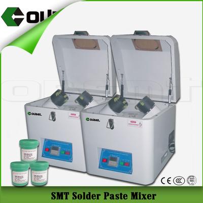
New Equipment | Solder Paste Mixers
Unique contoured shape, generous appearance and practical, which is made by advanced coating process workmanship. Mixing principle is on the basis of Motor rotation and revolution mode of agitation, no need to defrost the paste. Need to recovery the
Industry News | 2018-10-18 08:27:03.0
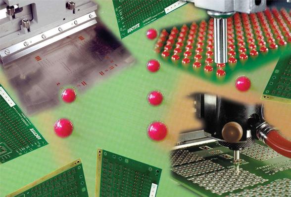
An Analysis of SMT Solder Paste Printing Defects
Industry News | 2018-10-18 09:56:07.0
What are the Factors Affecting the Cost of PCB Production?
As the first commercially available adhesive to address the emerging surface-mount market in the 1980s, Loctite Chip bonder and Eccobond products today are the industry standard for mixed-technology and double-sided surface mount technology (SMT) app
Technical Library | 2023-03-16 18:51:43.0
Conductive anodic filament (CAF) formation was first reported in 1976.1 This electrochemical failure mode of electronic substrates involves the growth of a copper containing filament subsurface along the epoxy-glass interface, from anode to cathode. Despite the projected lifetime reduction due to CAF, field failures were not identified in the 1980s. Recently, however, field failures of critical equipment have been reported.2 A thorough understanding of the nature of CAF is needed in order to prevent this catastrophic failure from affecting electronic assemblies in the future. Such an understanding requires a comprehensive evaluation of the factors that enhance CAF formation. These factors can be grouped into two types: (1) internal variables and (2) external influences. Internal variables include the composition of the circuit board material, and the conductor metallization and configuration (i.e. via to via, via to surface conductor or surface conductors to surface conductors). External influences can be due to (1) production and (2) storage and use. During production, the flux or hot air solder leveling (HASL) fluid choice, number and severity of temperature cycles, and the method of cleaning may influence CAF resistance. During storage and use, the principal concern is moisture uptake resulting from the ambient humidity. This paper will report on the relationship between these various factors and the formation of CAF. Specifically, we will explore the influences of printed wiring board (PWB) substrate choice as well as the influence of the soldering flux and HASL fluid choices. Due to the ever-increasing circuit density of electronic assemblies, CAF field failures are expected to increase unless careful attention is focused on material and processing choices.
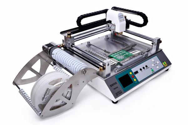
Application TM240A is widely used in 1. small batch production 2. product sample trials 3. PCB&LED SMT processing 4. other similar processes It is ideal choice for small medium manufacturing enterprises and research laboratories! Applicable P
Industry News | 2018-10-18 09:37:27.0
How To Set Profile In SMT Reflow Oven
Technical Library | 2020-10-18 19:35:05.0
Interconnect reliability especially in BGA solder joints and compliant pins are subjected to design parameters which are very critical to ensure product performance at pre-defined shipping condition and user environment. Plating thickness of compliant pin and damping mechanism of electronic system design are key successful factors for this purpose. In additional transportation and material handling process of a computer server system will be affected by shock under certain conditions. Many accessories devices in the server computer system tend to become loose resulting in poor contact or solder intermittent interconnect problems due to the shock load from the transportation and material handling processes.


