
Used SMT Equipment | In-Circuit Testers
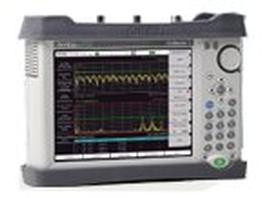
Anritsu S331E Base Frequency: 20 MHz Max Frequency: 4 GHz Anritsu S331E Sitemaster - Anritsu is pleased to introduce its eighth-generation compact handheld Site Master cable and antenna analyzer series with integrated spectrum analyzer. The new S

Used SMT Equipment | In-Circuit Testers
Anritsu S331E Base Frequency: 20 MHz Max Frequency: 4 GHz Anritsu S331E Sitemaster - Anritsu is pleased to introduce its eighth-generation compact handheld Site Master cable and antenna analyzer series with integrated spectrum analyzer. The new S

Used SMT Equipment | In-Circuit Testers
Anritsu S331E Base Frequency: 20 MHz Max Frequency: 4 GHz Anritsu S331E Sitemaster - Anritsu is pleased to introduce its eighth-generation compact handheld Site Master cable and antenna analyzer series with integrated spectrum analyzer. The new S

Used SMT Equipment | In-Circuit Testers
Anritsu S331E Base Frequency: 20 MHz Max Frequency: 4 GHz Anritsu S331E Sitemaster - Anritsu is pleased to introduce its eighth-generation compact handheld Site Master cable and antenna analyzer series with integrated spectrum analyzer. The new S
Used SMT Equipment | In-Circuit Testers
Anritsu S331E Base Frequency: 20 MHz Max Frequency: 4 GHz Anritsu S331E Sitemaster - Anritsu is pleased to introduce its eighth-generation compact handheld Site Master cable and antenna analyzer series with integrated spectrum analyzer. The new S
Career Center | Ogdensburg, New York | Engineering
To monitor and continually improve manufacturing processes by leading projects targeting quality, improving service, generating growth and improving the overall productivity of business operations by utilizing lean/6-sigma tools. ? Lead, identify
Technical Library | 2014-10-30 01:48:43.0
The ultimate life of a microelectronics component is often limited by failure of a solder joint due to crack growth through the laminate under a contact pad (cratering), through the intermetallic bond to the pad, or through the solder itself. Whatever the failure mode proper assessments or even relative comparisons of life in service are not possible based on accelerated testing with fixed amplitudes, or random vibration testing, alone. Effects of thermal cycling enhanced precipitate coarsening on the deformation properties can be accounted for by microstructurally adaptive constitutive relations, but separate effects on the rate of recrystallization lead to a break-down in common damage accumulation laws such as Miner's rule. Isothermal cycling of individual solder joints revealed additional effects of amplitude variations on the deformation properties that cannot currently be accounted for directly. We propose a practical modification to Miner's rule for solder failure to circumvent this problem. Testing of individual solder pads, eliminating effects of the solder properties, still showed variations in cycling amplitude to systematically reduce subsequent acceleration factors for solder pad cratering. General trends, anticipated consequences and remaining research needs are discussed
Industry News | 2018-01-16 11:59:10.0
Vision Engineering has teamed up with industry-expert Bob Willis to broadcast a free Electronics Academy Webinar aimed at identifying the issues affecting PCB/SMT assembly and the challenges of achieving Zero Defect Manufacture. The next webinar, Eliminate Printed Circuit Board Problems & Failure Modes will take place on January 23rd at 2:30 EST.
Technical Library | 2020-07-08 20:05:59.0
There is a compelling need for functional testing of high-speed input/output signals on circuit boards ranging from 1 gigabit per second (Gbps) to several hundred Gbps. While manufacturing tests such as Automatic Optical Inspection (AOI) and In-Circuit Test (ICT) are useful in identifying catastrophic defects, most high-speed signals require more scrutiny for failure modes that arise due to high-speed conditions, such as jitter. Functional ATE is seldom fast enough to measure high-speed signals and interpret results automatically. Additionally, to measure these adverse effects it is necessary to have the tester connections very close to the unit under test (UUT) as lead wires connecting the instruments can distort the signal. The solution we describe here involves the use of a field programmable gate array (FPGA) to implement the test instrument called a synthetic instrument (SI). SIs can be designed using VHDL or Verilog descriptions and "synthesized" into an FPGA. A variety of general-purpose instruments, such as signal generators, voltmeters, waveform analyzers can thus be synthesized, but the FPGA approach need not be limited to instruments with traditional instrument equivalents. Rather, more complex and peculiar test functions that pertain to high-speed I/O applications, such as bit error rate tests, SerDes tests, even USB 3.0 (running at 5 Gbps) protocol tests can be programmed and synthesized within an FPGA. By using specific-purpose test mechanisms for high-speed I/O the test engineer can reduce test development time. The synthetic instruments as well as the tests themselves can find applications in several UUTs. In some cases, the same test can be reused without any alteration. For example, a USB 3.0 bus is ubiquitous, and a test aimed at fault detection and diagnoses can be used as part of the test of any UUT that uses this bus. Additionally, parts of the test set may be reused for testing another high-speed I/O. It is reasonable to utilize some of the test routines used in a USB 3.0 test, in the development of a USB 3.1 (running at 10 Gbps), even if the latter has substantial differences in protocol. Many of the SI developed for one protocol can be reused as is, while other SIs may need to undergo modifications before reuse. The modifications will likely take less time and effort than starting from scratch. This paper illustrates an example of high-speed I/O testing, generalizes failure modes that are likely to occur in high-speed I/O, and offers a strategy for testing them with SIs within FPGAs. This strategy offers several advantages besides reusability, including tester proximity to the UUT, test modularization, standardization approaching an ATE-agnostic test development process, overcoming physical limitations of general-purpose test instruments, and utilization of specific-purpose test instruments. Additionally, test instrument obsolescence can be overcome by upgrading to ever-faster and larger FPGAs without losing any previously developed design effort. With SIs and tests scalable and upward compatible, the test engineer need not start test development for high-speed I/O from scratch, which will substantially reduce time and effort.
Technical Library | 2024-09-02 18:48:58.0
The conversion to higher temperature "Lead Free" assembly reflow conditions has created an increased awareness that entrapped or absorbed moisture is a frequent root cause of thermally induced delamination at assembly reflow. There are two connected failure modes from entrapped moisture; incomplete resin cross-linking resulting in premature resin decomposition and also severe Z axis expansion from "explosive vaporization of the entrapped moisture at elevated temperatures at assembly reflow". Ultimately, both result in delamination failure. Other papers have shown the negative effects of entrapped moisture before lamination including delamination, red color, reduced thermal reliability and increased high speed signal loss. In this paper, various materials were tested for moisture sensitivity during lamination. Tests were performed at varying lamination conditions including a pre-vacuum step and "kiss" step. Pressure and cure temperature parameters were evaluated for minimizing or eliminating the effect of trapped moisture. Also included are the results of inner layer moisture removal baking conditions and their effect on peel strength and thermal reliability.


.gif)
