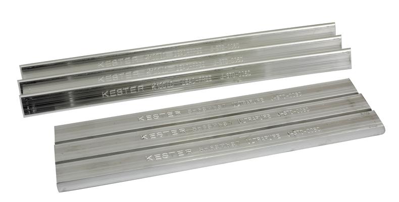
New Equipment | Solder Materials
Manufactured by a special process that controls the inclusions of oxides and metallic and non-metallic impurities, Kester Ultrapure® is the industry standard bar solder for use in high tech electronic applications where lower surface tension and hole
Industry Directory | Manufacturer
Manufacturer of sintering, electrically conductive materials. Applications include semiconductor die attach, component attach, via fill, z-axis interconnection, conductive lines and traces and plated-through hole fill.
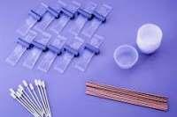
New Equipment | Coating Materials
This kit contains 10 packages of clear, low viscosity, superior strength epoxy, precisely measured out into two-compartment plastic packages so it's easy to use and there's no measuring. Once cured, this epoxy makes an effective electrical insulator
Technical Library | 2019-06-26 23:21:49.0
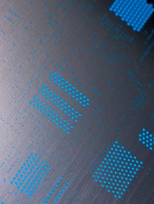
Copper-filled micro-vias are a key technology in high density interconnect (HDI) designs that have enabled increasing miniaturization and densification of printed circuit boards for the next generation of electronic products. Compared with standard plated through holes (PTHs) copper filled vias provide greater design flexibility, improved signal performance, and can potentially help reduce layer count, thus reducing cost. Considering these advantages, there are strong incentives to optimize the via filling process. This paper presents an innovative DC acid copper via fill formulation, for VCP (Vertical Continues Plating) applications which rapidly fills vias while minimizing surface plating.
New Equipment | Education/Training
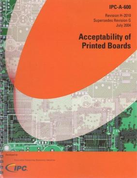
IPC A-600H Acceptability of Electronic Assemblies. The IPC-A-600, "Acceptability of Printed Boards " is the most widely used published specification on printed wiring boards. This specification has set the standard for rigid printed boards in terms o
Industry Directory | Manufacturer
UWELLPCB.com is the PCB supplier. We offer PCB from single side board, double side PCB to 32layer board,including the Rigid PCB, Flex PCB, Rigid-flex PCB,Quick-turn prototype and PCB assembly
New Equipment | Solder Paste Stencils
Lasercut LTCC-stencil (Low Temperature Cofired Ceramic) The LTCC-technology (low temperature co-fired ceramic) is used in the hybrid-technique when several interconnection levels are realized. The connections between the layers are manufactured with
With the development of miniaturization of assembly components, the layout area and pattern design area of PCBs have also been continuously reduced, and PCB manufacturers are constantly updating the production process to conform to the development tr
Industry News | 2010-09-08 11:49:17.0
PCB Fabricator Installs MASS VHF 300 VS for Via Hole Filling Addressing the continuous demands pertaining to via hole filling, through holes and blind vias
New Equipment | Solder Materials
Lead-free wave and selective soldering systems require exposing the flux to slightly higher soldering temperatures. Lead-free alloys traditionally wet metal surfaces more slowly than tin-lead. Kester liquid fluxes for lead-free assembly have new acti


