Technical Library | 2019-07-17 17:56:34.0
The increased demand for electronic devices in recent years has led to an extensive research in the field to meet the requirements of the industry. Electrolytic copper has been an important technology in the fabrication of PCBs and semiconductors. Aqueous sulfuric acid baths are explored for filling or building up with copper structures like blind micro vias (BMV), trenches, through holes (TH), and pillar bumps. As circuit miniaturization continues, developing a process that simultaneously fills vias and plates TH with various sizes and aspect ratios, while minimizing the surface copper thickness is critical. Filling BMV and plating TH at the same time, presents great difficulties for the PCB manufactures. The conventional copper plating processes that provide good via fill and leveling of the deposit tend to worsen the throwing power (TP) of the electroplating bath. TP is defined as the ratio of the deposit copper thickness in the center of the through hole to its thickness at the surface. In this paper an optimization of recently developed innovative, one step acid copper plating technology for filling vias with a minimal surface thickness and plating through holes is presented.
Industry Directory | Consultant / Service Provider / Manufacturer
Manufacturer of highly miniaturized and high reliability PCBs. Swiss Quality substrates for demanding applications such as implants and medical devices. HDI flex, rigid-flex and rigid PCBs in small to medium volumes.
Technical Library | 2024-07-24 01:27:58.0
A study of the Thermo Design PCB Indicates The better the performance of the heatsink (=low Rth), the more influence the TIMs have The thickness of a TIM is often more critical than the thermal conductivity of the material The thermal resistance of the surface between the materials are most critical Better use many small vias than a few big vias! Plated or filled vias are very expensive to get, better try to stay with standard!
New Equipment | Solder Paste Stencils
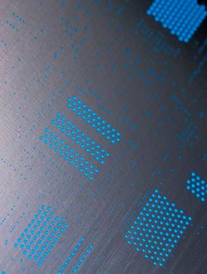
Lasercut LTCC-stencil (Low Temperature Cofired Ceramic) The LTCC-technology (low temperature co-fired ceramic) is used in the hybrid-technique when several interconnection levels are realized. The connections between the layers are manufactured with
Industry Directory | Manufacturer
A printed circuit board manufacturer producing high quality prototype printed circuit boards.
Industry Directory | Manufacturer
We specialize in Flex PCBs, Ridgid Flex, Long Flex PCBs and RF (radio frequency) Boards. Our engineering team has seen it all.
Technical Library | 2011-02-17 18:03:21.0
Copper ground pours are created by filling open unused areas with copper generally on the outer layers of the board then connecting the copper fill with stitching vias to ground. Usually, small isolated areas
Technical Library | 2021-05-26 00:53:26.0
This paper describes a copper electroplating enabling technology for filling microvias. Driven by the need for faster, smaller and higher performance communication and electronic devices, build-up technology incorporating microvias has emerged as a viable multilayer printed circuit manufacturing technology. Increased wiring density, reduced line widths, smaller through-holes and microvias are all attributes of these High Density Interconnect (HDI) packages. Filling the microvias with conductive material allows the use of stacked vias and via in pad designs thereby facilitating additional packaging density. Other potential design attributes include thermal management enhancement and benefits for high frequency circuitry. Electrodeposited copper can be utilized for filling microvias and provides potential advantages over alternative via plugging techniques. The features, development, scale up and results of direct current (DC) and periodic pulse reverse (PPR) acid copper via filling processes, including chemistry and equipment, are described.
Industry Directory | Manufacturer
Manufacturer of sintering, electrically conductive materials. Applications include semiconductor die attach, component attach, via fill, z-axis interconnection, conductive lines and traces and plated-through hole fill.
Training Courses | ON DEMAND | | IPC-600 Trainer (CIT)
The Certified IPC-600 Trainer (CIT) courses recognize individuals as qualified trainers in the area of quality assurance of bare printed circuit boards and prepare them to deliver Certified IPC-600 (CIS) training.
winsouce.jpg)


