Technical Library | 2020-07-15 18:29:34.0
In the early 2000s the first fine-pitch ball grid array devices became popular with designers looking to pack as much horsepower into as small a space as possible. "Smaller is better" became the rule and with that the mechanical drilling world became severely impacted by available drill bit sizes, aspect ratios, and plating methodologies. First of all, the diameter of the drill needed to be in the 0.006" or smaller range due to the reduction of pad size and spacing pitch. Secondly, the aspect ratio (depth to diameter) became limited by drill flute length, positional accuracy, rigidity of the tools (to prevent breakage), and the throwing power of acid copper plating systems. And lastly, the plating needed to close up the hole as much as possible, which led to problems with voiding, incomplete fill, and gas/solution entrapment.
Technical Library | 2019-10-10 00:26:28.0
Voids are a plague to our electronics and must be eliminated! Over the last few years we have studied voiding in solder joints and published three technical papers on methods to "Fill the Void." This paper is part four of this series. The focus of this work is to mitigate voids for via in pad circuit board designs. Via holes in Quad Flat No-Lead (QFN) thermal pads create voiding issues. Gasses can come out of via holes and rise into the solder joint creating voids. Solder can also flow down into the via holes creating gaps in the solder joint. One method of preventing this is via plugging. Via holes can be plugged, capped, or left open. These via plugging options were compared and contrasted to each other with respect to voiding. Another method of minimizing voiding is through solder paste stencil design. Solder paste can be printed around the via holes with gas escape routes. This prevents gasses from via holes from being trapped in the solder joint. Several stencil designs were tested and voiding performance compared and contrasted. In many cases voiding will be reduced only if a combination of mitigation strategies are used. Recommendations for combinations of via hole plugging and stencil design are given. The aim of this paper is to help the reader to "Fill the Void."

New Equipment | Fabrication Services
RF & Microwave PCB's ACI is a leader in providing complex RF/Microwave PCB’s covering a wide spectrum of product types including Defense/Aerospace, Medical Device, Imaging, and Telecommunications Equipment. ACI supports a wide range of frequency ban
Industry News | 2003-03-11 09:04:04.0
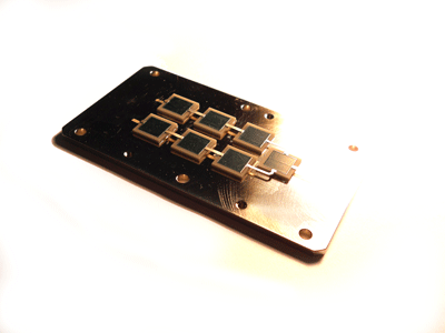
Developed in response to customer requirements, the new Via Fill process from DEK delivers 100% fill of substrate vias with no voids and minimal surface residue.
Technical Library | 2014-11-13 19:23:50.0
With increasing power loss of electrical components, thermal performance of an assembled device becomes one of the most important quality factors in electronic packaging. Due to the rapid advances in semiconductor technology, particularly in the regime of high-power components, the temperature dependence of the long-term reliability is a critical parameter and has to be considered with highest possible care during the design phase (...) The aim of this paper is to give a short overview about standard thermal solutions like thick copper, thermal vias, plugged vias or metal core based PCBs. Furthermore, attention will be turned on the development of copper filled thermal vias in thin board constructions...
Technical Library | 2021-06-21 19:34:02.0
In this era of electronics miniaturization, high yield and low-cost integrated circuit (IC) substrates play a crucial role by providing a reliable method of high density interconnection of chip to board. In order to maximize substrate real-estate, the distance between Cu traces also known as line and space (L/S) should be minimized. Typical PCB technology consists of L/S larger than 40 µ whereas more advanced wafer level technology currently sits at or around 2 µm L/S. In the past decade, the chip size has decreased significantly along with the L/S on the substrate. The decreasing chip scales and smaller L/S distances has created unique challenges for both printed circuit board (PCB) industry and the semiconductor industry. Fan-out panel-level packaging (FOPLP) is a new manufacturing technology that seeks to bring the PCB world and IC/semiconductor world even closer. While FOPLP is still an emerging technology, the amount of high-volume production in this market space provide a financial incentive to develop innovative solutions in order to enable its ramp up. The most important performance aspect of the fine line plating in this market space is plating uniformity or planarity. Plating uniformity, trace/via top planarity, which measures how flat the top of the traces and vias are a few major features. This is especially important in multilayer processing, as nonuniformity on a lower layer can be transferred to successive layers, disrupting the device design with catastrophic consequences such as short circuits. Additionally, a non-planar surface could also result in signal transmission loss by distortion of the connecting points, like vias and traces. Therefore, plating solutions that provide a uniform, planar profile without any special post treatment are quite desirable.
Industry Directory | Consultant / Service Provider / Manufacturer
BBG will service your quick turn prototype, your small volume run as well as your full production requirement. We have plants dedicated to quick turn, small volume and prototype applications.
At Barry: custom requests are common and welcome. We enjoy the challange. Extensive capabilities, wide material selection and state-of-the-art equiptment (including in-house plating and machining) ensure we can deliver a component fitting your exact
Technical Library | 2020-07-22 19:39:05.0
The PWB industry needs to complete reliability testing in order to define the minimum copper wrap plating thickness requirement for confirming the reliability of PTH structures. Predicting reliability must ensure that the failure mechanism is demonstrated as a wear-out failure mode because a plating wrap failure is unpredictable. The purpose of this study was to quantify the effects of various copper wrap plating thicknesses through IST testing followed by micro sectioning to determine the failure mechanism and identify the minimum copper wrap thickness required for a reliable PWB. Minimum copper wrap plating thickness has become an even a bigger concern since designers started designing HDI products with buried vias, microvias and through filled vias all in one design. PWBs go through multiple plating cycles requiring planarization after each plating cycle to keep the surface copper to a manageable thickness for etching. The companies started a project to study the relationship between Copper wrap plating thickness and via reliability. The project had two phases. This paper will present findings from both Phase 1 and Phase 2.
IPC 6012 Qualification and Performance Specification for Rigid Printed Boards This specification covers qualification and performance of rigid PCBs including with or without plated-through holes, single-sided, double-sided, multilayer with or withou


.gif)
winsouce.jpg)