
Innovative Materials, Superior Performance. Our printed circuit board and semiconductor packaging materials provide superior thermal and mechanical performance, a fact we’ve prided ourselves on for over 45 years. All our materials are RoHS complian
Industry News | 2019-11-05 22:08:21.0
Via in pad is the design practice of placing a via in the copper landing pad of a component. Compared to standard PCB via routing, via in pad allows a design to use smaller component pitch sizes and further reduce the PCBs overall size. With component manufactures pushing smaller parts every year and the demand from consumers for smaller devices, the usage of via in pad practices by hardware engineers have become more commonplace. In this article, we will discuss the differences between via in pad and traditional vias, when should you use via in pad, and how to design for it.
Technical Library | 2022-12-05 16:28:06.0
The work evaluates the impact of latent heat (LH) absorbed or released by a solder alloy during melting or solidification, respectively, on changes of dimensions of materials surrounding of the solder alloy. Our sample comprises a small printed circuit board (PCB) with a blind via filled with lead-free alloy SAC305. Differential scanning calorimetry (DSC) was employed to obtain the amount of LH per mass and a thermomechanical analyzer was used to measure the thermally induced deformation. A plateau during melting and a peak during solidification were detected during the course of dimension change. The peak height reached 1.6 μm in the place of the heat source and 0.3 μm in the distance of 3 mm from the source. The data measured during solidification was compared to a numerical model based on the finite element method. An excellent quantitative agreement was observed which confirms that the transient expansion of PCB during cooling can be explained by the release of LH from the solder alloy during solidification. Our results have important implications for the design of PCB assemblies where the contribution of recalescence to thermal stress can lead to solder joint failure.

This video describes the IPC A-600 training and certification program. The IPC A-600 specification is a set of acceptability specifications for printed circuit boards. These standards determine the acceptance and reject criteria for printed wiring bo
Technical Library | 2016-11-03 17:53:56.0
We present a novel method for fabricating a high-density carbon nanotube microelectrode array (MEA) chip. Vertically aligned carbon nanotubes (VACNTs) were synthesized by microwave plasma-enhanced chemical vapor deposition and thermal chemical vapor deposition. The device was characterized using electrochemical experiments such as cyclic voltammetry, impedance spectroscopy and potential transient measurements. Through-silicon vias (TSVs) were fabricated and partially filled with polycrystalline silicon to allow electrical connection from the high-density electrodes to a stimulator microchip.In response to the demand for higher resolution implants, we have developed a unique process to obtain a high-density electrode array by making the microelectrodes smaller in size and designing new ways of routing the electrodes to current sources.
With the development of miniaturization of assembly components, the layout area and pattern design area of PCBs have also been continuously reduced, and PCB manufacturers are constantly updating the production process to conform to the development tr
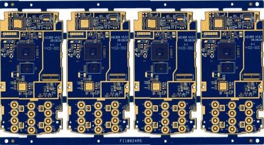
High-density interconnection/HDI PCB Layer: 8 (HDI) Structure: 2+4+2 with stack via Material: FR4(Tg170) Thiness: 1.0mm Surface treatment: Selective immersion gold + OSP Blind via L1-2 & L2-3 & L6-7 & L7-8: 0.1MM (4mil) Buried via L3-6:

SIPAD Systems Incorporated (SSi) is the Exclusive Supplier of SIPAD solid solder deposit in North America and the only SIPAD Solid Solder Deposit (SSD) coating service bureau in the world. SIPAD Systems Inc. supplies SIPAD solid solder coating servi
Industry News | 2019-11-05 22:07:01.0
Tenting a via refers to covering via with soldermask to enclose or skin over the opening. A via is a hole drilled into the PCB that allows multiple layers on the PCB to be connected to each other. A non tented via is just a via that is not covered with the soldermask layer. Leaving these vias exposed or covered has pros and cons depending on the your design and manufacturing requirements.
Industry News | 2012-06-11 22:12:24.0
Colonial Circuits has acquired an ESI 5200 Laser as an integral part of upgrading their facility to handle the highest technology products including Micro and Stacked vias.


