New Equipment | Education/Training
IPC J-STD 001 REV F Requirements for Soldered Electrical and Electronic Assemblies. The IPC J-STD-001F standard is the industry-consensus document with respect to the assembly of PCBs and electronic assemblies. Released August 2014. IPC J-STD-001
New Equipment | Assembly Services
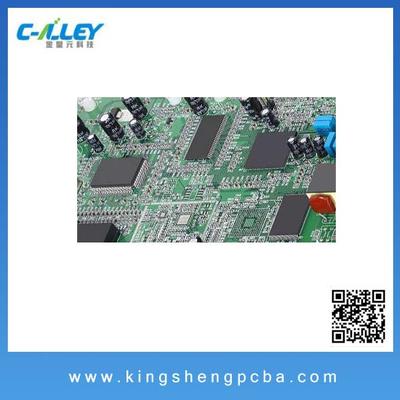
Our Service PCB Assembly and PCB&PCBA design are our main business.We are able to undertake a high quality Printed Circuit Board Assembly on competitive prices and flexible conditions.We are a complete “One- Stop” resource for printed circuit board
Technical Library | 2021-09-29 13:35:21.0
In PCB circuit assemblies the trend is moving to more SMD components with finer pitch connections. The majority of the assemblies still have a small amount of through hole (THT) components. Some of them can't withstand high reflow temperatures, while others are there because of their mechanical robustness. In automotive applications these THT components are also present. Many products for cars, including steering units, radio and navigation, and air compressors also use THT technology to connect board-to-board, PCB's to metal shields or housings out of plastic or even aluminium. This is not a simple 2D plain soldering technology, as it requires handling, efficient thermal heating and handling of heavy (up to 10 kg) parts. Soldering technology becomes more 3D where connections have to be made on different levels. For this technology robots using solder wire fail because of the spattering of the flux in the wires and the long cycle time. In wave soldering using pallets the wave height is limited and pin in paste reflow is only a 2D application with space limitations. Selective soldering using dedicated plates with nozzles on the solder area is the preferred way to make these connections. All joints can be soldered in one dip resulting in short cycle times. Additional soldering on a small select nozzle can make the system even more flexible. The soldering can only be successful when there is enough thermal heat in the assembly before the solder touches the board. A forced convection preheat is a must for many applications to bring enough heat into the metal and board materials. The challenge in a dip soldering process is to get a sufficient hole fill without bridging and minimize the number of solder balls. A new cover was designed to improve the nitrogen environment. Reducing oxygen levels benefits the wetting, but increases the risk for solder balling. Previous investigations showed that solder balling can be minimized by selecting proper materials for solder resist and flux.
Technical Library | 2020-09-02 22:02:13.0
With the adoption of Wafer Level Packages (WLP) in the latest generation mobile handsets, the Printed Circuit Board (PCB) industry has also seen the initial steps of High Density Interconnect (HDI) products migrating away from the current subtractive processes towards a more technically adept technique, based on an advanced modified Semi Additive Process (amSAP). This pattern plate process enables line and space features in the region of 20um to be produced, in combination with fully filled, laser formed microvias. However, in order to achieve these process demands, a step change in the performance of the chemical processes used for metallization of the microvia is essential. In the electroless Copper process, the critical activator step often risks cross contamination by the preceding chemistries. Such events can lead to uncontrolled buildup of Palladium rich residues on the panel surface, which can subsequently inhibit etching and lead to short circuits between the final traces. In addition, with more demands being placed on the microvia, the need for a high uniformity Copper layer has become paramount, unfortunately, as microvia shape is often far from ideal, the deposition or "throw" characteristics of the Copper bath itself are also of critical importance. This "high throwing power" is influential elsewhere in the amSAP technique, as it leads to a thinner surface Copper layer, which aids the etching process and enables the ultra-fine features being demanded by today's high end PCB applications. This paper discusses the performance of an electroless Copper plating process that has been developed to satisfy the needs of challenging amSAP applications. Through the use of a radical predip chemistry, the formation, build up and deposition of uncontrolled Pd residues arising from activator contamination has been virtually eradicated. With the adoption of a high throwing power Copper bath, sub 30um features are enabled and microvia coverage is shown to be greatly improved, even in complex via shapes which would otherwise suffer from uneven coverage and risk premature failure in service. Through a mixture of development and production data, this paper aims to highlight the benefits and robust performance of the new electroless Copper process for amSAP applications
Industry News | 2008-03-25 23:22:33.0
Comment from Neil O�Brien, Director � US Sales
Industry News | 2019-11-05 22:08:21.0
Via in pad is the design practice of placing a via in the copper landing pad of a component. Compared to standard PCB via routing, via in pad allows a design to use smaller component pitch sizes and further reduce the PCBs overall size. With component manufactures pushing smaller parts every year and the demand from consumers for smaller devices, the usage of via in pad practices by hardware engineers have become more commonplace. In this article, we will discuss the differences between via in pad and traditional vias, when should you use via in pad, and how to design for it.
Industry News | 2018-01-04 14:47:35.0
Kurtz Ersa North America announces that it has appointed Technical Resources Corporation (TRC) as its manufacturers’ representative in Florida. TRC will represent and sell Ersa’s complete line of equipment.
Industry News | 2018-01-08 18:11:29.0
Kurtz Ersa North America announces that it has appointed Technical Resources Corporation (TRC) as its manufacturers’ representative in Florida. TRC will represent and sell Ersa’s complete line of equipment.
Industry News | 2010-09-20 19:43:37.0
Registrations for the webinar launch of DEK’s new ProActiv technology are escalating. With just over a week to go, keen interest is being shown by hundreds of participants signing up from Europe, Asia and the Americas.
Industry News | 2008-05-03 16:43:51.0
One of the UK's leading design and manufacturers of standard and bespoke microwave component technology has invested in new machinery at its Presteigne microwave printed circuit board (PCB) production facility, with the aim of improving processes, efficiency and manufacturing capability.


