Training Courses | | | PCB Design Courses
The PCB design courses teach students the process, techniques and tools needed to design layout of printed circuit boards.
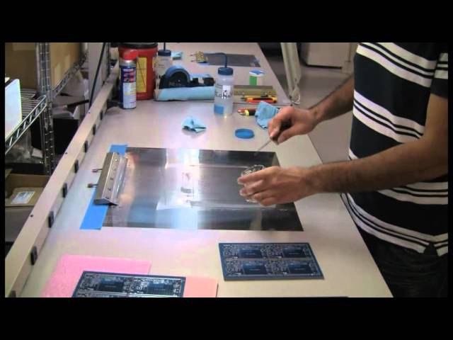
This is video shows how to print a PCB using a prototype foil only stencil. The SMT prototype stencil (www.soldertools.net) is made from a high nickel content material able to offer repeatable high precision apertures. The steps of alignment, printin
This is video shows how to print a PCB using a prototype foil only stencil. The SMT prototype stencil (www.soldertools.net) is made from a high nickel content material able to offer repeatable high precision apertures. The steps of alignment, printin
Industry News | 2016-02-27 20:41:52.0
BEST Inc. instructors will be conducting 2 training sessions this year at the APEX Expo 2016 - Advanced Rework: Hands-on BGA Reballing, Lead-Free Devices, and Fine-Pitch Parts, and the 2nd session - Stencil Printing: Consistent Print Volumes for SMT Rework.

Do you have issues with the height of your paste deposit when printing close to your clamp foils? Let SigmaPrint take you to the EDGE of your printing boundaries! The CustomFoil � (PAT APP FOR) board clamp replacement system from SigmaPrint Technolog
Designers and fabricators are always arguing about how to reduce track width and increase reliability of the circuitry. One effective solution is MicroThin�. MicroThin� is a very low profile copper 3�m or 5�m copper foil with an 18�m or 35�m peelable
New Equipment | Solder Paste Stencils
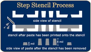
Stentech has the technical ability to manufacture step stencils in both single process and dual process. Today's complex PCBs with the various components require different solder paste volumes. Stentech has the technical expertise to optimize the ste
Industry Directory | Manufacturer
Manufacturer of Laser Cut & Chemical Etched Stencils.
Technical Library | 2020-09-02 22:14:36.0
The demand for miniaturization and higher density electronic products has continued steadily for years, and this trend is expected to continue, according to various semiconductor technology and applications roadmaps. The printed circuit board (PCB) must support this trend as the central interconnection of the system. There are several options for fine line circuitry. A typical fine line circuit PCB product using copper foil technology, such as the modified semi-additive process (mSAP), uses a thin base copper layer made by pre-etching. The ultrathin copper foil process (SAP with ultrathin copper foil) is facing a technology limit for the miniaturization due to copper roughness and thickness control. The SAP process using sputtered copper is a solution, but the sputtering process is expensive and has issues with via plating. SAP using electroless copper deposition is another solution, but the process involved is challenged to achieve adequate adhesion and insulation between fine-pitch circuitries. A novel catalyst system--liquid metal ink (LMI)--has been developed that avoids these concerns and promotes a very controlled copper thickness over the substrate, targeting next generation high density interconnect (HDI) to wafer-level packaging substrates and enabling 5-micron level feature sizes. This novel catalyst has a unique feature, high density, and atomic-level deposition. Whereas conventional tin-palladium catalyst systems provide sporadic coverage over the substrate surface, the deposited catalyst covers the entire substrate surface. As a result, the catalyst enables improved uniformity of the copper deposition starting from the initial stage while providing higher adhesion and higher insulation resistance compared to the traditional catalysts used in SAP processes. This article discusses this new catalyst process, which both proposes a typical SAP process using the new catalyst and demonstrates the reliability improvements through a comparison between a new SAP PCB process and a conventional SAP PCB process.
Industry Directory | Consultant / Service Provider / Manufacturer
One of the major suppliers of stencils and pallets to the SMT industry. Stentech offers Electroformed and laser cut stencils, pallets and fixtures.


