Industry News | 2014-06-03 13:04:15.0
The OneChip Photonics facility in Kanata; Ontario, Canada will be closing their site and all assets are being sold via an online auction. The bidding for the auction will open promptly at 4:00am EST on June 3, 2014 with Lots 1-512 beginning to close at 11am EST on June 4, 2014.
Training Courses | | | PCB Assembly Courses
The PCB assembly courses provide knowledge of different processes and equipment used in TH and SMT assembly of printed circuit boards.
Parts & Supplies | Pick and Place/Feeders
RETROFIT KIT F.FLIP CHIP SENSOR
Technical Library | 2019-05-21 17:34:08.0
Flip chip components have been gaining popularity in the electronics industry since their introduction in the 1960s. Advances in attach methods and adhesives, as well as the drive for smaller and faster electronic devices made the technology take off. The basic premise of the flip chip is that the chip (semiconductor device) is mounted flipped from the traditional position. The traditional method of mounting a die is to mount it on a lead frame with the circuit and bond pads face up. The bond pads then receive a bond wire which then connects to the proper lead on the lead frame. Flip chips are mounted face down onto a substrate using small bumps on the bond pads to make direct electrical connection to their respective pads on the substrate. Stay tuned for more information on attachment techniques next month. This article will focus on how to rework flip chips.
Technical Library | 2019-05-21 17:38:55.0
Last month we presented Flip Chip Rework.As promised, this month we follow up with attachment techniques. Flip chip assembly is a key technology for advanced packaging of microelectronic circuits. It allows attachment of a bare chip to a packaging substrate in a face-down configuration, with electrical connections between the chip and substrate via conducting “bumps.” Flip chip technology was first invented by IBM for mainframe computer application in the early 1960s. Semiconductor devices are mounted face down and electrically and mechanically connected to a substrate (Figure 1). IBM called this manufacturing process a C4 process (controlled collapse chip connection).
Training Courses | | | PCB Design Courses
The PCB design courses teach students the process, techniques and tools needed to design layout of printed circuit boards.
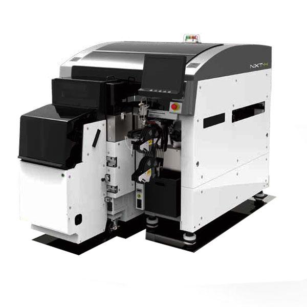
Used SMT Equipment | Chipshooters / Chip Mounters
NXT-H and NXT-Hw support placing small LEDs and bare dies at high-speed as well as performing hybrid production including flip chips.Fuji Ultra Accurate Placement Platform.Hybrid placement of wafers and SMDs. Wafer and reel part placement in a single
Events Calendar | Mon Apr 12 00:00:00 EDT 2021 - Mon Apr 12 00:00:00 EDT 2021 | ,
Europe Chapter Webinar: Tombstoning Components during Reflow Soldering - Causes & Cures
_1.jpg)
SMT Samsung CP feeder 8x2mm, PA-NST for 01005 pick and place machine Samsung SM/CP40 CP45 Feeders models: SAMSUNG SM 8*2mm FEEDER SAMSUNG SM 8*4mm FEEDER SAMSUNG SM 12mm FEEDER SAMSUNG SM 16mm FEEDER SAMSUNG SM 24mm FEEDER SAMSUNG SM 32mm FEEDER SAM


