
Industry Directory | Consultant / Service Provider / Media / Publisher / Online Resource / Other
PCB Libraries' "Footprint Expert" suite uses CAD LEAP(tm) Technology to greatly simplify footprint and 3D STEP model creation; it is used by tens of thousands of PCB designers and engineers all over the world.
Industry Directory | Consultant / Service Provider
SnapEDA is the Internet's first parts library for circuit board design, providing free symbols, footprints and 3D models for millions of electronic components. Join half a million engineers at www.snapeda.com.
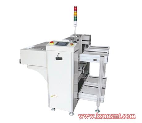
New Equipment | Board Handling - Conveyors
product instruction ※PLC control system, Working is stably and reliably ※Easy to operate touch screen control interface ※the pneumatic clamps of top and bottom three point provided for the magazine alignment ※Electric pushing board design ca

New Equipment | Board Handling - Conveyors
product instruction ※PLC control system, Working is stably and reliably ※Easy to operate touch screen control interface ※the pneumatic clamps of top and bottom three point provided for the magazine alignment ※Electric pushing board design ca
Electronics Forum | Tue Jun 03 12:49:29 EDT 2008 | operator
If only my company would pay for a membership to IPC......
Electronics Forum | Wed Jun 04 00:13:18 EDT 2008 | operator
Very informative article. Thanks Dave.

Used SMT Equipment | Soldering - Reflow
Still running production unit new unit delivered before the end of the year. The Heller 1809 MK5 is a reflow soldering system used in electronics manufacturing. Here are some key specifications and features: Model: 1809 MK5 Heating Zones: 9 Zones
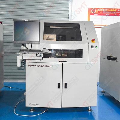
Used SMT Equipment | Screen Printers
Momentum was designed and built to be a no-nonsense production machine. Cost-efficient and featuring a modest footprint, it grows with the user; innovative patented features can be added on or retrofitted as needed as the user’s throughput dema
Industry News | 2016-06-22 15:33:28.0
Based on its recent analysis of the surface mount technology (SMT) reflow soldering equipment market, Frost & Sullivan recognizes Heller Industries, Inc. with the 2016 Global Frost & Sullivan Award for Growth Excellence Leadership. Heller Industries has made remarkable improvements to its product and technology portfolios over the last 10 years to emerge a top participant in the SMT reflow soldering equipment market.
Industry News | 2017-08-19 13:31:56.0
GPD Global will demonstrate its Hyperion dispense system in booths 1C03 & 1C10 at upcoming NEPCON South China 2017. This fully automated dispense platform incorporates the latest technology from GPD Global in a compact footprint. Equipped with linear motor drives, smart pump technology, full touch screen interface, vision centric system operation & more, this is a dispense system not to be missed.
 – pn 51305433.jpg)
Parts & Supplies | Pick and Place/Feeders
0402 Ceramic Blade Nozzle (3030) – p/n 51305433 You might ask, “What’s the difference between this nozzle and the older conical 0402 ceramic nozzle?” Simply put, we think this latest design is a far superior option. Here&
 51305434_1.jpg)
Parts & Supplies | Pick and Place/Feeders
0603 Ceramic Blade Nozzle 3040 51305434 We were so impressed with the new long-life ceramic 0402 nozzle (#3030) we launched earlier in 2014 that we decided to follow it up with an 0603 version! Now customers can reap the benefits of our ESD-Safe ce
Technical Library | 2010-11-06 02:44:38.0
An increasing number of video equipment is running at Gigabit rates today. They are interconnected through relatively large size coaxial BNC connectors. While these connectors are in general of good quality, their performance in the equipment depends on
Technical Library | 2018-09-26 20:33:26.0
Bottom terminated components, or BTCs, have been rapidly incorporated into PCB designs because of their low cost, small footprint and overall reliability. The combination of leadless terminations with underside ground/thermal pads have presented a multitude of challenges to PCB assemblers, including tilting, poor solder fillet formation, difficult inspection and – most notably – center pad voiding. Voids in large SMT solder joints can be difficult to predict and control due to the variety of input variables that can influence their formation. Solder paste chemistries, PCB final finishes, and reflow profiles and atmospheres have all been scrutinized, and their effects well documented. Additionally, many of the published center pad voiding studies have focused on optimizing center pad footprint and stencil aperture designs. This study focuses on I/O pad stencil modifications rather than center pad modifications. It shows a no-cost, easily implemented I/O design guideline that can be deployed to consistently and repeatedly reduce void formation on BTC-style packages.

The PCB Footprint Expert is a powerful CAD library development tool powered by our own proprietary CAD LEAP Technology (Libraries Enhanced with Automated Preferences). It is packed with very powerful advanced library management features that cuts foo
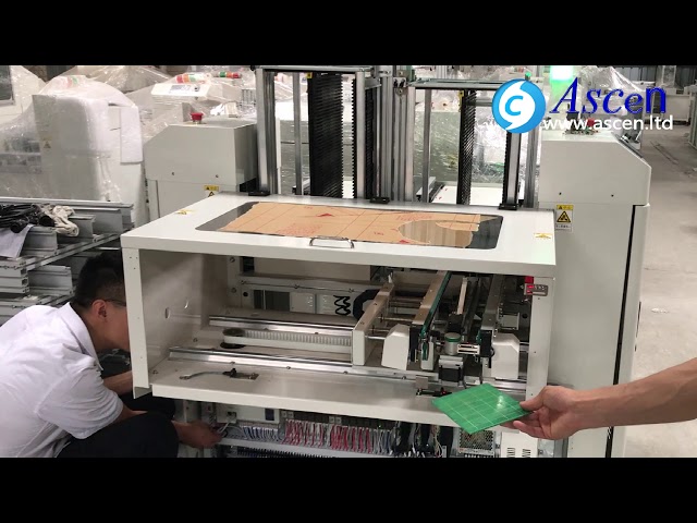
NG OK pcb magazine unloader|PCB NG OK unloader or double track magazine PCB unloader after AOI machine, receive the signal given by AOI https://www.ascen.ltd/Products/Automatic_SMT_equipment/PCB_loader/131.html ASCEN major for the PCB conveyor and t
Training Courses | | | PCB Design Courses
The PCB design courses teach students the process, techniques and tools needed to design layout of printed circuit boards.
Training Courses | | | PCB Assembly Courses
The PCB assembly courses provide knowledge of different processes and equipment used in TH and SMT assembly of printed circuit boards.
Events Calendar | Mon Jun 10 00:00:00 EDT 2024 - Mon Jun 10 00:00:00 EDT 2024 | Carlsbad, California USA
San Diego Chapter In-Person Event: IPC J-STD-001 Compliant Solder Pattern Calculations for DFA
Events Calendar | Thu Mar 18 00:00:00 EDT 2021 - Thu Mar 18 00:00:00 EDT 2021 | ,
India Chapter Webinar: PCBA Process Qualifications
Career Center | Clarksburg, Maryland USA | Engineering,Management,Research and Development,Technical Support
We are currently seeking a Senior Manufacturing Engineer for our Clarksburg, Maryland location. The candidate must be driven with a strong ability to multi-task under pressure. Responsibilities: The successful candidate will be responsible for:
Career Center | San Jose, CA, California USA | Engineering,Production,Research and Development
Senior PCB Designer: Want to be part of an exciting pre-IPO enterprise B2B company working on the cutting edge of internet-of-things, artificial intelligence & agents, blockchain, and manufacturing technology? This well-funded venture-backed co
Career Center | Newport Beach, California USA | Engineering,Management,Production
KEVIN RAGER P.O.BOX 7878, NEWPORT BEACH, 949 922 8997, KEVIN.RAGER@EDA-INC.US OBJECTIVE I am trying to find a consistent work flow that provides mentally challenging yet stimulating experiences in design and prototype development. EXPERIENCE 1997
| https://www.eptac.com/blog/3-common-pcb-design-mistakes
3 Common PCB Design Mistakes Looking for solder training standards, manuals, kits, and more? Visit soldertraining.com Training Training Materials Locations Resources Ask Helena
| https://pcbasupplies.com/small-footprint-dry-cabinet-302-series/
Small Footprint Dry Cabinet Login Create Account Contact View My Cart Menu × Categories Hand Soldering & Rework Automation Tooling PCB Support Systems Soldering Robots Material Handling Dry Storage Cabinets Component Handling Selective Solder Nozzles Pick


