
Layer: 2 Material: FR-4 Board Thickness: 1.6mm Surface Finish: HAL Copper Thickness: 2/2 oz Green Solder Mask Layers: 2--36layers Max manufacturing size: 640mm*1100mm Copper foil thickness: 0.5OZ-13OZ Min line width/space: 3mil/3mil Min
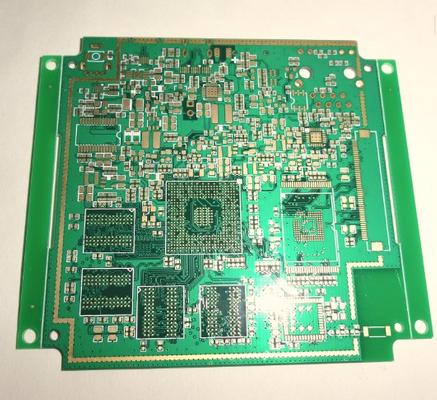
Layer: 6 layers Material: FR-4 Board Thickness: 1.0mm Surface Finish:ENIG Copper Thickness: 1 oz all layers Blind via L1~L2 and L1~L3 Layers: 2--36layers Max manufacturing size: 640mm*1100mm Copper foil thickness: 0.5OZ-13OZ Min line width
Technical Library | 2023-08-04 15:27:30.0
A designed experiment evaluated the influence of several variables on appearance and strength of Pb-free solder joints. Components, with leads finished with nickel-palladium-gold (NiPdAu), were used from Texas Instruments (TI) and two other integrated circuit suppliers. Pb-free solder paste used was tin-silver-copper (SnAgCu) alloy. Variables were printed wiring board (PWB) pad size/stencil aperture (the pad finish was consistent; electrolysis Ni/immersion Au), reflow atmosphere, reflow temperature, Pd thickness in the NiPdAu finish, and thermal aging. Height of solder wetting to component lead sides was measured for both ceramic plate and PWB soldering. A third response was solder joint strength; a "lead pull" test determined the maximum force needed to pull the component lead from the PWB. This paper presents a statistical analysis of the designed experiment. Reflow atmosphere and pad size/stencil aperture have the greatest contribution to the height of lead side wetting. Reflow temperature, palladium thickness, and preconditioning had very little impact on side-wetting height. For lead pull, variance in the data was relatively small and the factors tested had little impact.
Technical Library | 2024-04-08 15:46:36.0
A designed experiment evaluated the influence of several variables on appearance and strength of Pb-free solder joints. Components, with leads finished with nickel-palladium-gold (NiPdAu), were used from Texas Instruments (TI) and two other integrated circuit suppliers. Pb-free solder paste used was tin-silver-copper (SnAgCu) alloy. Variables were printed wiring board (PWB) pad size/stencil aperture (the pad finish was consistent; electrolysis Ni/immersion Au), reflow atmosphere, reflow temperature, Pd thickness in the NiPdAu finish, and thermal aging. Height of solder wetting to component lead sides was measured for both ceramic plate and PWB soldering. A third response was solder joint strength; a "lead pull" test determined the maximum force needed to pull the component lead from the PWB. This paper presents a statistical analysis of the designed experiment. Reflow atmosphere and pad size/stencil aperture have the greatest contribution to the height of lead side wetting. Reflow temperature, palladium thickness, and preconditioning had very little impact on side-wetting height. For lead pull, variance in the data was relatively small and the factors tested had little impact.
Technical Library | 2015-11-25 14:15:12.0
In this study various printed circuit board surface finishes were evaluated, including: organic solderability preservative (OSP), plasma finish (PF), immersion silver (IAg), electroless nickel / immersion silver (ENIS), electroless nickel / immersion gold hi-phosphorus (ENIG Hi-P), and electroless nickel / electroless palladium / immersion gold (ENEPIG). To verify the performance of PF as a post-treatment option, it was added to IAg, ENIG Hi-P, and ENEPIG to compare with non-treated. A total of nine groups of PCB were evaluated. Each group contains 30 boards, with the exception on ENIS where only 8 boards were available.
New Equipment | Assembly Services
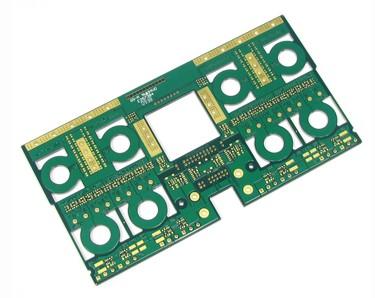
PCB process capability Base material: CM1, CM3, FR1, FR4, Metal based Layer: 1 to 24 layers Board thickness: 0.4mm to 3mm Copper thickness: 0.5oZ, 1oZ, 2oZ Min Copper thickness in hole: 0.02mm Max working size: 400*610mm Surface finishing: HAS
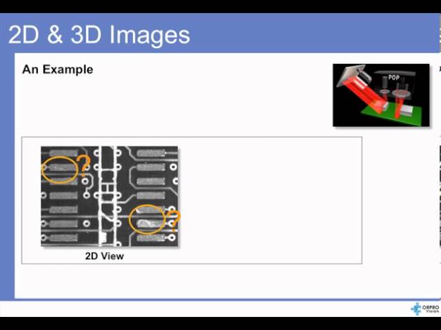
ORPRO Vision SPI Presentation. This presentation introduces the methods and technology used by ORPRO Vision in the Symbion P36 Plus SPI system. For additional information, please contact ORPRO Vision at sales.us@orprovision.com sales.eu@orprovision
Technical Library | 2014-11-06 16:43:24.0
This paper summarizes the results of recent investigations to examine the effect of electroless nickel process variations with respect to Pb-free (Sn-3.0Ag-0.5Cu) solder connections. These investigations included both ENIG and NiPd as surface finishes intended for second level interconnects in BGA applications. Process variations that are suspected to weaken solder joint reliability, including treatment time and pH, were used to achieve differences in nickel layer composition. Immersion gold deposits were also varied, but were directly dependent upon the plated nickel characteristics. In contrast to gold, different electroless palladium thicknesses were independently achieved by treatment time adjustments.
Industry News | 2011-08-19 05:08:40.0
Nickel gold is one of the most popular surface finishes used in the PCB assembly industry with many advantages but also process and reliability issues.
New Equipment | Design Services
Layer:4 Material:FR-4 4/4/4/4oz Thickness:2.0 Minimum hole:0.35mm Minimum Tracc/Spacing:12mil/15mil Application:power supply Layers: 2--36layers Max manufacturing size: 640mm*1100mm Copper foil thickness: 0.5OZ-13OZ Min line width/space:
.png)


