Industry News | 2018-03-13 18:47:01.0
TopLine will once again be the premier sponsor of the upcoming IMAPS Wire Bonding Conference. In making the announcement, TopLine CEO Martin Hart stated that he is delighted to support the conference as the leading sponsor for the second time. The Wire Bonding workshop and tabletop exhibition will be held October 8, 2018 in California at the Pasadena Convention Center. The event is co-located with the IMAPS 51st Symposium on Microelectronics.
Industry Directory | Consultant / Service Provider
Supermax ECAD - Advanced EDA solutions for PCB, MCM & Hybrid design. Supports all types of designs including RF, Microwave, High-Speed and Advanced Packaging.
Industry News | 2018-10-18 11:08:03.0
Different Techniques for Plating
Industry News | 2013-10-31 11:53:09.0
Hesse GmbH will demonstrate a full range of wedge wire bonding capabilities at Productronica, taking place November 12-15 in Munich, Germany, in Hall B2, Booth 255.
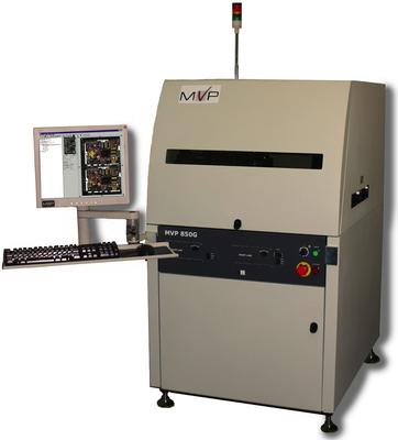
Microelectronics and Semiconductor Inspection. MVP's 850G provides the highest accuracy flip-chip, die assembly inspection. Ensuring the correct placement of the die on the substrate, while providing edge, FM and surface inspection. The 850G modu
Industry News | 2010-02-19 09:45:37.0
Pressurex® Sensor Film Needed to Measure Contact Pressure In Ultrasonic Welding
Parts & Supplies | Circuit Board Assembly Products
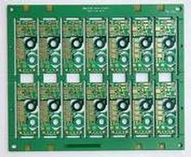
PULANG TECHNOLOGY CO,.LTDOffers electronic manufacturing services including PCB designing, electronic contract manufacturing including electronic product design, electronic product development, electronic product repair, PCB manufacturing, electronic
Industry News | 2015-08-11 09:37:25.0
Saline Lectronics now offers wire bonding in-house as an added-value service. With the installation of the Kulicke & Soffa 4500 Manual Wedge Bonder, Saline Lectronics is now one of the only electronic contract manufacturers in the Midwest to support wire bonding services.
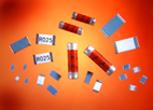
Welwyn Components� new SMT facility contains the latest manufacturing techniques for both standard and specialist chip resistors. These include high speed/ high precision printing and lasering equipment, grading and tape packing machines and a state
Welwyn Components� new SMT facility contains the latest manufacturing techniques for both standard and specialist chip resistors. These include high speed/ high precision printing and lasering equipment, grading and tape packing machines and a state


