Technical Library | 2019-04-10 22:08:31.0
The stimulating impact of the automotive industry has sharpened focus on immersion tin (i-Sn) more than ever before. Immersion tin with its associated attributes, is well placed to fulfill the requirements of such a demanding application. In an environment dominated by reliability, the automotive market not only has very stringent specifications but also demands thorough qualification protocols. Qualification is ultimately a costly exercise. The good news is that i-Sn is already qualified by many tier one OSATs. The focus of this paper is to generate awareness of the key factors attributed to soldering i-Sn. Immersion tin is not suitable for wire bonding but ultimately suited for multiple soldering applications. The dominant topics of this paper will be IMC formations in relation to reflow cycles and the associated solderability performance. Under contamination free conditions, i-Sn can provide a solderable finish even after multiple reflow cycles. The reflow conditions employed in this paper are typical for lead free soldering environments and the i-Sn thicknesses are approximately 1 μm.
Industry News | 2011-04-06 13:13:52.0
Dow Electronic Materials will showcase its innovative materials for printed circuit boards (PCBs) at this year’s IPC APEX EXPO. Dow will feature a number of its latest products that are tailored to meet the requirements of increasingly complex circuit boards while delivering ever-higher reliability and consistency. Dow’s next-generation of high quality, cost-effective technologies allow customers to meet future market requirements.
Industry News | 2013-06-07 14:37:14.0
Hesse Mechatronics will introduce and demonstrate the new Bondjet BJ931L in booth 6081 in the North Hall at SEMICON West, taking place July 9-11 in San Francisco.
Technical Library | 2023-08-04 15:27:30.0
A designed experiment evaluated the influence of several variables on appearance and strength of Pb-free solder joints. Components, with leads finished with nickel-palladium-gold (NiPdAu), were used from Texas Instruments (TI) and two other integrated circuit suppliers. Pb-free solder paste used was tin-silver-copper (SnAgCu) alloy. Variables were printed wiring board (PWB) pad size/stencil aperture (the pad finish was consistent; electrolysis Ni/immersion Au), reflow atmosphere, reflow temperature, Pd thickness in the NiPdAu finish, and thermal aging. Height of solder wetting to component lead sides was measured for both ceramic plate and PWB soldering. A third response was solder joint strength; a "lead pull" test determined the maximum force needed to pull the component lead from the PWB. This paper presents a statistical analysis of the designed experiment. Reflow atmosphere and pad size/stencil aperture have the greatest contribution to the height of lead side wetting. Reflow temperature, palladium thickness, and preconditioning had very little impact on side-wetting height. For lead pull, variance in the data was relatively small and the factors tested had little impact.
Technical Library | 2024-04-08 15:46:36.0
A designed experiment evaluated the influence of several variables on appearance and strength of Pb-free solder joints. Components, with leads finished with nickel-palladium-gold (NiPdAu), were used from Texas Instruments (TI) and two other integrated circuit suppliers. Pb-free solder paste used was tin-silver-copper (SnAgCu) alloy. Variables were printed wiring board (PWB) pad size/stencil aperture (the pad finish was consistent; electrolysis Ni/immersion Au), reflow atmosphere, reflow temperature, Pd thickness in the NiPdAu finish, and thermal aging. Height of solder wetting to component lead sides was measured for both ceramic plate and PWB soldering. A third response was solder joint strength; a "lead pull" test determined the maximum force needed to pull the component lead from the PWB. This paper presents a statistical analysis of the designed experiment. Reflow atmosphere and pad size/stencil aperture have the greatest contribution to the height of lead side wetting. Reflow temperature, palladium thickness, and preconditioning had very little impact on side-wetting height. For lead pull, variance in the data was relatively small and the factors tested had little impact.
Industry News | 2014-05-07 16:11:10.0
AI Technology (AIT) Releases Electrically and Thermally Conductive 20 Micron Wafer Level Die-Attach Film (DAF), Combines High Glass Transition Temperature and Stress Absorption with Proven Thermal Performance in Die-Attach Power Dissipation.
Industry News | 2003-05-05 09:13:55.0
Reliable Wire Bonders for High Yield Production
For flip chip attachment or electrical grounding ACP's for Electrical Interconnection Zymet's ACP’s designed for electrical interconnection are used for flip chip attachment. Applications include chip-on-glass (COG) attachment of driver IC's and
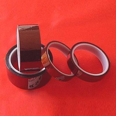
Polyimide tape can either be amber or clear in color, and the film thickness ranges 1 and 3 mils while the adhesive may range from 1 to 2 mils thick. It may be double sided, and the adhesive may be silicone or acrylic based. Anti-static Polyimide t
Industry News | 2024-01-29 11:36:51.0
Indium Corporation® will feature its high-reliability, Au-based precision die-attach (PDA) preforms for critical laser and RF applications at SPIE Photonics West, Jan. 27-Feb. 1, in San Francisco. SPIE West is the world's premier event for lasers, biomedical optics and biophotonic technologies, quantum, and optoelectronics.


