Industry Directory | Consultant / Service Provider
CAD Design Software products run in the AutoCAD environment.
Industry Directory | Consultant / Service Provider
A printed circuit board design service bureau located in the great Pacific Northwest. We specialize in large, complex, fast turn designs common in the video processing and data processing industries.
We have tremendous experience in using various software tools to meet your project requirements. During the development of your product, we work closely with your electrical engineers and mechanical engineers to ensure that the placement of the part
EPD is the base system. Its tools automate PCB design. Parts are parametrically created and stored. The Place command searches libraries and loads parts into the netlist. Colored dynamically optimized rats aid parts placement. Routing with on-line
Electronics Forum | Fri Jun 16 10:38:33 EDT 2000 | Iain
I have 15 very large backplanes (.156" thick Au plating) that the ground pins of a high density thru-hole connector were not thermal relieved in the artwork. As a result we are unable to solder the 8 pins that connect to the ground plane. We know t
Electronics Forum | Wed Apr 18 14:17:48 EDT 2018 | esoderberg
Further divide the ground block into more than 4 panes. Also think about using, assuming you have good placement of using Loctite chip bonder on two opposing corners. Lots of ways to get good results
Industry News | 2011-11-03 21:52:00.0
By davef: I was fortunate to be able to attend the SMTAI Exhibition Oct. 18-19, 2011. While I was walking around looking at the booths and talking to the exhibitors, I got this idea that I would report back on things that I found interesting. You know spread the news, since not everyone was there.
Industry News | 2003-03-11 08:45:00.0
CAMtastic DXP is the latest version of Altium's complete CAM verification and editing system that bridges the gap between PCB design and manufacturing and facilitates communication between board designers, fabrication engineers, and their clients.
Technical Library | 2019-05-21 17:20:36.0
Die attach material selection and process implementation play crucial roles in any microelectronic assembly. The chosen attach methods ultimately affect die stress, functionality, thermal management, and reliability of the assembly. Die attach applications are designed to optimize mechanical attachment of the die to the substrate, to create a thermal path from the die to the substrate, and to create an electrical path for a ground plane connection. Some of the more commonly used die attach materials in the microelectronics industry today are epoxies,polyimides, thermoplastics, silicones, solders, and special low outgassing, low stress, anisotropic adhesives.
Technical Library | 2019-07-24 23:55:32.0
Voiding is a key concern for components with thermal planes because interruptions in Z-axis continuity of the solder joint will hinder thermal transfer. When assembling components with solder paste, there is a high propensity for voiding due to the confined nature of the solder paste deposits under the component. Once reflowed, many factors contribute to the amount of voiding in a solder joint such as the reflow profile, designs of the component, board and stencil, and material factors. This study will focus on the solder paste alloy and flux combination as well as profile and board surface finishes.

ACI Technologies Inc. (ACI) is a scientific research corporation dedicated to the advancement of electronics manufacturing processes and materials for The Department of Defense and industry. This video provides an overview of our commercial service
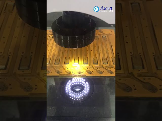
https://www.ascen.ltd/Products/PCB_board_assembly_system/vision_measurin/507.html Vision Measuring Machine and image measuring instrument can be used for dimensional accuracy measurement of various molds, aircraft, automobile, mobile phone, computer,
Career Center | Auckland, New Zealand | Engineering
NAVMAN PCBA NPI Engineer Reporting To: PCBA NPI Technical Leader Primary Objective: Transition of PCBs from R&D design to a manufacturable state conforming to all facets of PCBA production Secondary: Develop DFM & best practice guidelines Res
Career Center | Beaumont, Michigan, Minnesota, Canada USA | Engineering
Infrared camera electronics design and camera design engineer. Manage electronic design, research and development, optimize current design, manage prototype design, fabrication and testing. Some optical design experience is preferred, but not not nec
Career Center | THRISSUR, India | Maintenance,Production
HANDLING OF MAINTENANCE Camelot,Mascot, Selective Soldering,Wave Soldering,Aquastorm 200,H-500 HI-Z,Kolb,kerry&PBT,GETECH, ATI 105 & Final Touch 101,Heller,Btu&vapour phase,Shuttle,SRT,ESD ,Electrical maintenance . Knowledge in using SLIM KIC 2000&
| https://www.smtfactory.com/How-to-prevent-static-electricity-during-the-operation-of-the-Full-auto-SMT-Production-Line-id3182659.html
Series Reflow Oven LV Series Vacuum Reflow Oven SMT Stencil Printing Machine Semi-auto SMT Stencil Printer Full-auto SMT Stencil Printer Pick
| http://etasmt.com/cc?ID=te_news_bulletin,25362&url=_print
temperature profiles Description: The Ersa HOTFLOW 4/26 Reflow Soldering System is of robust design and manufactured entirely from steel, welded air-tight, powder coated and with interior electric cabinet and a PC operating terminal
.jpg)


