Industry Directory | Manufacturer
Manufacturer of UV cure coatings and adhesives for the electronics and microelectronics industries. Materials include new 100% solids "B" staged UV cure epoxy adhesives for sealing microelectronic packages.
Training Courses | | | IPC-7711/7721 Specialist (CIS)
The Certified IPC-7711/7721 Specialist (CIS) training focuses on rework of electronic assemblies and repair and modification of printed boards and electronic assemblies.
Training Courses | | | IPC-7711/7721 Trainer (CIT)
The Certified IPC-7711/7721 Trainer (CIT) courses recognize individuals as qualified trainers in the area of rework and repair of printed boards and electronic assemblies and prepares them to deliver Certified IPC-7711/7721 (CIS) training.
Up to 30 layers, down to 3 mil traces / spaces, 6 mil drilled holes. MIL-P-55110 approved for FR-4, polyimide, PTFE, epoxy Thermount(tm). Copper Sealed Vias are available. Deliveries down to 24 hours are available.
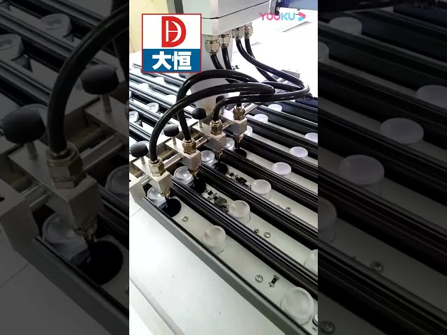
Wall washer potting machine Whatsapp 0086 134 2516 4065 online wall washer lap glue dispensing machine/AB glue dispensing machine/ hard led bar glue dispensing machine Applicable glue: One-component silicone, glass glue; two-component silicon

Sono-Tek's Selective Fluxing Systems provide excellent fine-line control and through-hole penetration for maximizing top-side fill. Compatible with all fluxes, our non-clogging ultrasonic nozzle technology is known worldwide as the industry standard
Technical Library | 2021-06-21 19:34:02.0
In this era of electronics miniaturization, high yield and low-cost integrated circuit (IC) substrates play a crucial role by providing a reliable method of high density interconnection of chip to board. In order to maximize substrate real-estate, the distance between Cu traces also known as line and space (L/S) should be minimized. Typical PCB technology consists of L/S larger than 40 µ whereas more advanced wafer level technology currently sits at or around 2 µm L/S. In the past decade, the chip size has decreased significantly along with the L/S on the substrate. The decreasing chip scales and smaller L/S distances has created unique challenges for both printed circuit board (PCB) industry and the semiconductor industry. Fan-out panel-level packaging (FOPLP) is a new manufacturing technology that seeks to bring the PCB world and IC/semiconductor world even closer. While FOPLP is still an emerging technology, the amount of high-volume production in this market space provide a financial incentive to develop innovative solutions in order to enable its ramp up. The most important performance aspect of the fine line plating in this market space is plating uniformity or planarity. Plating uniformity, trace/via top planarity, which measures how flat the top of the traces and vias are a few major features. This is especially important in multilayer processing, as nonuniformity on a lower layer can be transferred to successive layers, disrupting the device design with catastrophic consequences such as short circuits. Additionally, a non-planar surface could also result in signal transmission loss by distortion of the connecting points, like vias and traces. Therefore, plating solutions that provide a uniform, planar profile without any special post treatment are quite desirable.
This video describes the IPC A-600 training and certification program. The IPC A-600 specification is a set of acceptability specifications for printed circuit boards. These standards determine the acceptance and reject criteria for printed wiring bo
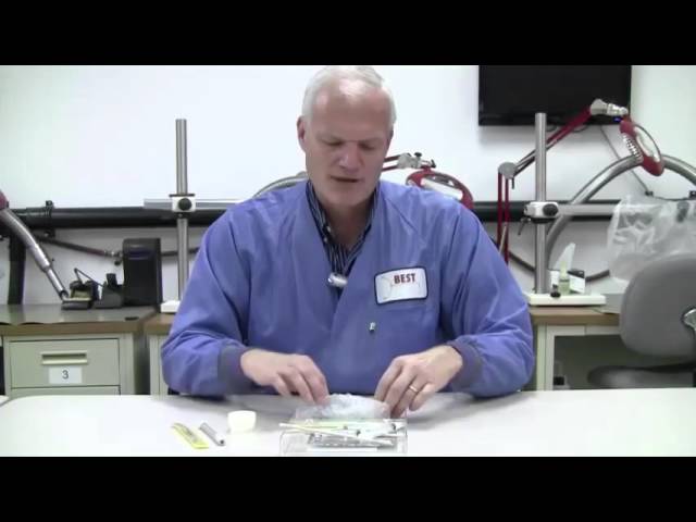
Poor handling procedures may sometimes damage corners and edges on printed circuit boards. Most of these types of damage to PCB's can be repaired using the BEST Board Repair Kit. This versatile repair kit along with our clear "how to" instructions of
Technical Library | 2013-10-31 17:36:41.0
Multilayer printed circuit boards (PCBs) that utilize high performance materials are inherently far more challenging for a fabricator to build, due to significant material property differences over standard epoxy glass FR4. These unique material characteristics often require higher processing temperatures, special surface treatments (to aid in hole and surface plating), they possess different expansion properties, making layer-to-layer registration more difficult to control, and require many other unique considerations.


