New Equipment | Solder Paste Stencils
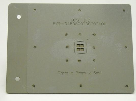
Based on its long work on BGA rework and repair process and its in-house capability to produce metal stencils BEST can provide for you a timely, cost-effective solution for printing on to components for MOST rework systems. Our templates for printin
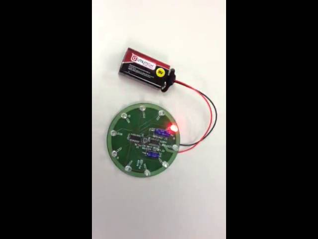
This is what the fully assembled How to Solder Kit looks like. Depress the button and one of the LEDs will remain lit at the end (it eventually times out). You can add some kind of template so each LED position has some meaning. The PCB has a real gr
New Equipment | Solder Paste Stencils
Eliminate hours of solder mask damage repair time for bga sites while improving rework yield. Are you frustrated by the time it takes to repair mask damage underneath the BGA during the rework process? Are you squeezed for space on the PCB in an
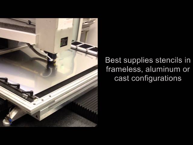
BEST manufactures and designs SMT stencils-both metal and plastic film type. This video demonstrates our metal stencil laser. See more on stencils here: http://www.soldertools.net/categories/Metal-Stencils/
BEST manufactures and designs SMT stencils-both metal and plastic film type. This video demonstrates our metal stencil laser. See more on stencils here: http://www.soldertools.net/categories/Metal-Stencils/
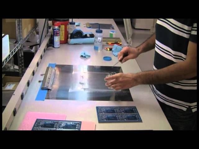
This is video shows how to print a PCB using a prototype foil only stencil. The SMT prototype stencil (www.soldertools.net) is made from a high nickel content material able to offer repeatable high precision apertures. The steps of alignment, printin
BEST manufactures and designs SMT stencils-both metal and plastic film type. This video demonstrates our metal stencil laser. See more on stencils here: http://www.soldertools.net/categories/Metal-Stencils/
This video presents the capabilities of BEST Inc in terms of its ability to perform high end PCB rework and repair services. BEST Inc., located in Rolling Meadows IL is a company of soldering "geeks". We rework/repair PCBs, train and certify solderin
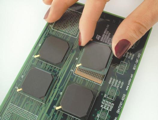
BGA integrated circuits and chip scale packages, CSPs where the solder connections are not visible. This has arisen as a result of the need for greater numbers of interconnections to integrated circuit packages and as a general result of increasing c

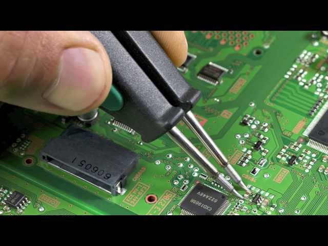
PCB pad repair technique demonstrated using the 2-part epoxy method. More on this PCB pad repair technique: http://www.solder.net/services/pcb-repair/pad-and-trace-repair/ More on the recommended epoxy: http://www.soldertools.net/pcb-repair-epoxy-r


