New Equipment | Design Services
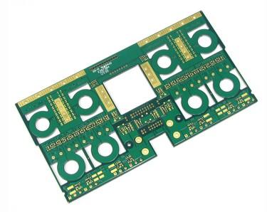
Layer:4 Material:FR-4 4/4/4/4oz Thickness:2.0 Minimum hole:0.35mm Minimum Tracc/Spacing:12mil/15mil Application:power supply Layers: 2--36layers Max manufacturing size: 640mm*1100mm Copper foil thickness: 0.5OZ-13OZ Min line width/space:

Layer: 2 Material: FR-4 Board Thickness: 1.6mm Surface Finish: HAL Copper Thickness: 2/2 oz Green Solder Mask Layers: 2--36layers Max manufacturing size: 640mm*1100mm Copper foil thickness: 0.5OZ-13OZ Min line width/space: 3mil/3mil Min
Layer: 6 layers Material: FR-4 Board Thickness: 1.0mm Surface Finish:ENIG Copper Thickness: 1 oz all layers Blind via L1~L2 and L1~L3 Layers: 2--36layers Max manufacturing size: 640mm*1100mm Copper foil thickness: 0.5OZ-13OZ Min line width
Industry News | 2021-06-30 04:24:18.0
Microtronic GmbH is pleased to introduce the new Automated & PC-Controlled D&L Automator for Dip and Look. Designed and manufactured in Germany, the new system meets IPC-J-STD-002 and 003 Standards.
Industry News | 2018-10-18 09:46:58.0
Analysis of how to spot welding process
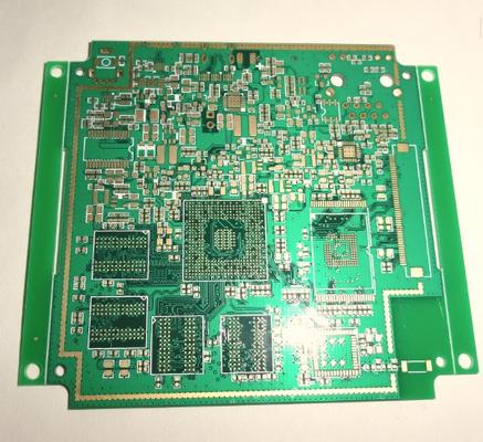
Double-Sided & Multi-Layer PCB Material: - FR-4 / Hi-Temp FR-4 / FR-5 / G10 / BT / Polyimide - Very Thin PCB: 0.004" 2L ~ 0.030" 8L - Thick Copper: 1/4 oz. ~ 11 oz. Process: - PTH - Blind/Buried/Segmented Via - Sequential Lamination - MicroVia Capa
Industry News | 2017-01-25 10:06:49.0
Register today for the 11th Annual International Electrostatic Workshop (IEW) being held May 7-11, 2017 at the Granlibakken Conference Center & Lodge, Lake Tahoe, CA USA The IEW facilitates access to and interactions with industry leaders through invited seminars, technical sessions, special interest groups (SIGs), discussion groups (DGs), and invited speakers. This year we focus on The Intersection of ESD Challenges for Emerging/Advancing Technologies and Markets; IC Designer’s Perspective on ESD; and Everything EOS – Product, Failure Analysis, Reliability, Verification, and Test Engineers. Participating at the IEW will provide: • An immersive, interactive experience with experts on technical advancements • All-inclusive pricing – workshop, hotel, and meals • Peer reviewed poster format for future full paper development • Gain valuable industry recognition and receive feedback • Interactive and in-depth discussion groups
Industry News | 2015-02-03 18:33:13.0
Panasonic Factory Solutions Company of America will premiere new hardware, application, and software solutions that amplify the depth and breadth of their total solutions for “Any Mix Any Volume” in booth 3539 at IPC APEX 2015.
Industry News | 2024-01-23 15:41:10.0
Koh Young Technology, the leader in True3D™ measurement-based inspection solutions, will be speaking at the SMTA Wafer-Level Packaging Symposium in Burlingame, California on our Multimodal Phase Shift Optics Approach to revolutionize high-speed 3D reconstruction of semiconductor and advanced packages. In the presentation will highlight how high-speed 3D reconstruction addresses the growing demand for electronic components, which necessitates fast and efficient processing. These advancements in measurement technology and AI integration have paved the way for enhanced packaging applications in the semiconductor industry.
Industry News | 2024-01-29 10:54:17.0
Koh Young Technology will be speaking at the SMTA Wafer-Level Packaging Symposium in Burlingame, California on our Multimodal Phase Shift Optics Approach to revolutionize high-speed 3D reconstruction of semiconductor and advanced packages. In the presentation will highlight how high-speed 3D reconstruction addresses the growing demand for electronic components, which necessitates fast and efficient processing. These advancements in measurement technology and AI integration have paved A machine with a computer on it Description automatically generatedthe way for enhanced packaging applications in the semiconductor industry.


