Industry News | 2003-04-10 10:27:46.0
IPC and JEDEC Send Out Call for Papers
Industry News | 2015-11-25 16:58:05.0
On behalf of the SMTA International Technical Committee, we invite you to submit a 300 word abstract of your research for the 2016 SMTA International 2016 technical conference in Rosemont, Illinois. Papers should describe significant results from experiments, emphasize new techniques, and contain technical, economic or appropriate test data. We are looking for papers on a variety of topics related to electronics manufacturing including advanced packaging/components, assembly, business/supply chain, emerging technologies, harsh environment applications, PCB technology, and process control. Materials must be original, unpublished and non-commercial in nature.
Industry Directory | Manufacturer
Supplier of high quality engineered materials, including conductive and resistive inks, UV curable dielectrics and insulators, adhesives, coatings, transducer inks and potting compounds.
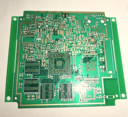
Layer: 8 layers Material: FR-4 Board Thickness: 0.6mm Surface Finish: Immersion Gold 1~4u Copper Thickness: 1/3 oz Impedance, 4/4mils width/spacing Layers: 2--36layers Max manufacturing size: 640mm*1100mm Copper foil thickness: 0.5OZ-13OZ M
Parts & Supplies | Circuit Board Assembly Products
PULANG TECHNOLOGY CO,.LTDOffers electronic manufacturing services including PCB designing, electronic contract manufacturing including electronic product design, electronic product development, electronic product repair, PCB manufacturing, electronic
New Equipment | Design Services
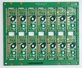
Layer:4 Material:FR-4 4/4/4/4oz Thickness:2.0 Minimum hole:0.35mm Minimum Tracc/Spacing:12mil/15mil Application:power supply Layers: 2--36layers Max manufacturing size: 640mm*1100mm Copper foil thickness: 0.5OZ-13OZ Min line width/space:

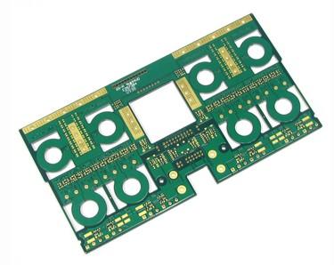
Layer: 2 Material: FR-4 Board Thickness: 1.6mm Surface Finish: HAL Copper Thickness: 2/2 oz Green Solder Mask Layers: 2--36layers Max manufacturing size: 640mm*1100mm Copper foil thickness: 0.5OZ-13OZ Min line width/space: 3mil/3mil Min
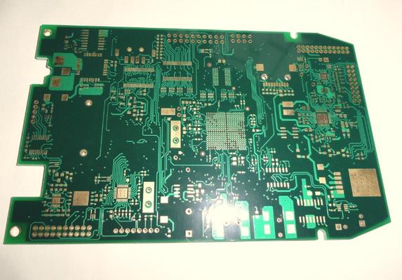
Layer: 6 layers Material: FR-4 Board Thickness: 1.0mm Surface Finish:ENIG Copper Thickness: 1 oz all layers Blind via L1~L2 and L1~L3 Layers: 2--36layers Max manufacturing size: 640mm*1100mm Copper foil thickness: 0.5OZ-13OZ Min line width
Technical Library | 2016-11-17 14:37:41.0
With increasing LED development and production, thermal issues are becoming more and more important for LED devices, particularly true for high power LED and also for other high power devices. In order to dissipate the heat from the device efficiently, Au80Sn20 alloy is being used in the industry now. However there are a few drawbacks for Au80Sn20 process: (1) higher soldering temperature, usually higher than 320°C; (2) low process yield; (3) too expensive. In order to overcome the shortcomings of Au80Sn20 process, YINCAE Advanced Materials, LLC has invented a new solderable adhesive – TM 230. Solderable adhesives are epoxy based silver adhesives. During the die attach reflow process, the solder material on silver can solder silver together, and die with pad together. After soldering, epoxy can encapsulate the soldered interface, so that the thermal conductivity can be as high as 58 W/mk. In comparison to Au80Sn20 reflow process, the solderable adhesive has the following advantages: (1) low process temperature – reflow peak temperature of 230°C; (2) high process yield – mass reflow process instead of thermal compression bonding process; (3) low cost ownership. In this paper we are going to present the die attach process of solderable adhesive and the reliability test. After 1000 h lighting of LED, it has been found that there is almost no decay in the light intensity by using solderable adhesive – TM 230.

SIPAD Systems Incorporated (SSi) is the Exclusive Supplier of SIPAD solid solder deposit in North America and the only SIPAD Solid Solder Deposit (SSD) coating service bureau in the world. SIPAD Systems Inc. supplies SIPAD solid solder coating servi


.jpg)

