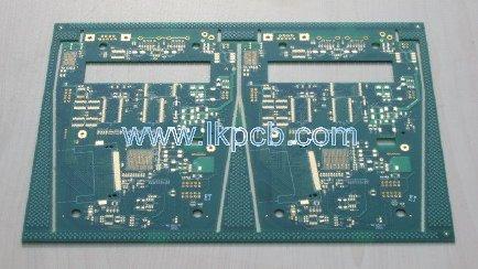
FR-4 Material 1.6 mm Thickness 12 Layers Immersion Gold Surface Treatment 0.2mm Drill Green Solder Mask Color BGA, Impedance Control
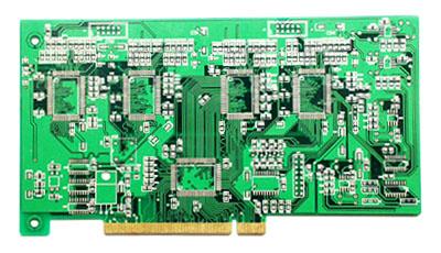
1. FR-4 Tg170 2. 20 layer, 1.6mm thick 3. 1 oz copper finished 4. 10% impedance control 5. Blind/buried vias 6. 0.1mm holes, HDI 7. Application: telecommunication, industrial control, medical equipment
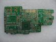
Gold finger PCB/Impedance computer circuit board Layer:6 Thiness: 2.0mm Surface treatment: ENIG+Hard gold plated on gold finger Impdance control: Single-ended 50ohm, differential 90 ohm Application: Computer
Technical Library | 2008-02-26 15:02:19.0
More and more chip packages need multi-GHz RF structures to meet their performance targets. The ideal chip package needs to combine RF features with Digital features for these applications. They drive low-loss, controlled impedance transmission lines, flexibility in assigned signal and power layers, and clearances of various shapes in power layers. Building these features in a chip package is difficult without making the stack-up very thick or compromising the reliability of the product. In the present paper, we have designed and built a flip-chip package test vehicle (TV) to make new RF structures, using Z-axis interconnection (Zinterconnect) building blocks.
Technical Library | 2009-07-09 17:23:07.0
Sometimes you just cannot clean with water. Good examples of this are: circuits with batteries attached, cleaning prior to encapsulation, ionic cleanliness testing, and non-sealed or other water sensitive parts. High impedance or high voltage circuits need to be cleaned of flux residues and other soils to maximize performance and reliability and, in these types of circuits; water can be just as detrimental as fluxes. When solvent cleaning is called for, Hansen solubility parameters can help target the best solvent or solvent blend to remove the residue of interest, and prevent degradation of the assembly being manufactured. In short, using this approach can time, manufacturing cost and reduce product liability.
Technical Library | 2016-11-03 17:53:56.0
We present a novel method for fabricating a high-density carbon nanotube microelectrode array (MEA) chip. Vertically aligned carbon nanotubes (VACNTs) were synthesized by microwave plasma-enhanced chemical vapor deposition and thermal chemical vapor deposition. The device was characterized using electrochemical experiments such as cyclic voltammetry, impedance spectroscopy and potential transient measurements. Through-silicon vias (TSVs) were fabricated and partially filled with polycrystalline silicon to allow electrical connection from the high-density electrodes to a stimulator microchip.In response to the demand for higher resolution implants, we have developed a unique process to obtain a high-density electrode array by making the microelectrodes smaller in size and designing new ways of routing the electrodes to current sources.
Technical Library | 2020-07-29 20:12:52.0
Aluminum is a metal that it is hard to solder due to the high surface tension difference between it and molten solder alloy. This occurs because aluminum rapidly forms a tenacious oxide layer whenever it is exposed to oxygen in the air. The oxide layer is responsible for the high surface tension difference between the aluminum and the solder and impedes the solder from spreading evenly on an aluminum surface. There are hundreds of aluminum alloys available in the marketplace; it is important to identify the form of aluminum that is being soldered. Once this is done, an appropriate soldering technique can be chosen for soldering the specific aluminum alloy under consideration. Direct aluminum soldering eliminates using expensive plating techniques to prepare the aluminum surface for soldering.
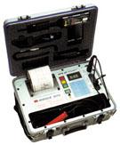
New Equipment | Test Equipment
This product is NEW USD $6960.00 Megger BITE 2 Megger Model # BITE 2 Catalog # 246002B Battery Impedance Test Equipment Determines condition of lead-acid and NiCd cells up to 7000 Ah On-board Pass/Warning/Fail indications Robust,
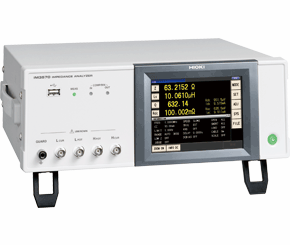
New Equipment | Test Equipment
Hioki IM3570 Impedance Analyzers $9995.00 IMPEDANCE ANALYZER IM3570 Single-device solution for high-speed measurement, even when switching between different measurement conditions The need to take readings of multiple parameters under d
PCB Design Service and CAE CAD CAM Training. Located in Colorado, our fast turn around PCB layout service has served customers coast-to-coast since 1990. Get your designs done quickly and without errors. Visit http://www.goldengategraphics.com.


