Technical Library | 2011-06-16 18:59:43.0
Based on tests carried out with commercially available chemistry, this paper discusses the advantages available through the use of NEAP processes for inner layer bonding and soldermask pretreatment. The process is characterized with a view to high volume
Events Calendar | Tue Jan 23 00:00:00 EST 2018 - Tue Jan 23 00:00:00 EST 2018 | New Milford, Connecticut USA
FREE Webinar: Eliminate Circuit Board Problems and Failure Modes
Parts & Supplies | Component Packaging
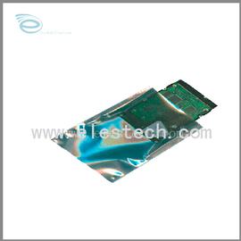
ES19101 ESD shielding bag ESD Shielding bags can utmostly protect sensitive components from potential static damage. Their special 4 layers structure forms an induction hood effect to isolate the inside items from electrostatic field. Besides, the
Technical Library | 2011-10-06 13:59:04.0
The desire to have more functionality into increasingly smaller size end products has been pushing the PCB and IC Packaging industry towards High Density Interconnect (HDI) and 3D Packaging (stacked dies, embedded packaged components). Many companies in the high-end consumer electronics market place have been embedding passive chip components on inner PCB and IC Packages for a few years now. However, embedding packaged components on inner layers has remained elusive for the broader market due to lack of proper design tools and high cost of embedding components on inner layers (...) This paper will highlight several key industrialization aspects addressed in the frame of the European funded FP7 HERMES* project to build a manufacturing environment for products with embedded components. The program entered its third year and is now dealing with the manufacturing of functional demonstrators as an introduction to industrialization.
Parts & Supplies | Tape and Reel
Product Description Pressure sensitive adhesive designed to adhere to both polystyrene and polycarbonate carrier tapes Excellent clarity Ultra smooth peel back Static dissipative on inner and outer layers All splice tape
Industry Directory | Manufacturer
professional manufacturer of pcb
Industry News | 2019-05-16 01:24:13.0
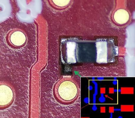
With the development of miniaturization of assembly components, the layout area and pattern design area of PCBs have also been continuously reduced, and PCB manufacturers are constantly updating the production process to conform to the development trend. The application of the resin plugging process has also become more and more extensive, and it has been used in HDI panels.
Industry News | 2015-01-20 23:40:52.0
Indium Corporation's Dr. Ning-Cheng Lee, vice president of technology, will present two SMTA webtorials on Feb. 10 and 17. Dr. Lee's presentation, Electromigration-The Hurdle for Miniaturization and High Power Devices, discusses critical aspects regarding the electromigration of solder joints, including failure mechanisms, the effect of solder alloy composition, solder joint metallurgy and configuration, pad design and composition, current density, temperature, and current polarity.
New Equipment | Rework & Repair Services
MLT provides laser rework services for PCB's including pad / component isolation and trace cutting. Contacts, pads, or other metal features can be laser defined or redimensioned without plunging into the dielectrics below. Trace cuts can be on the
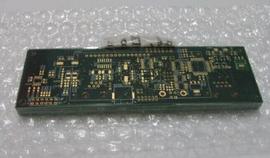
Parts & Supplies | Circuit Board Assembly Products
1) 160*100mm, FR-4 CTI ≥ 600V 2) 8 layer impedance control 3) Copper weight(finished inner/outer): 1 oz 4) LPI Green mask/white silk 5) Min hole 0.19mm, 5/3 track/gap 6) 1.6mm +/-10% thick 7) Immersiong gold over nickel


