
Industry Directory | Equipment Dealer / Broker / Auctions
Our Company handle AOI (Auto Optical Inspection) and SPI (Solder Paste Inspection) Machines.
Industry Directory | Manufacturer
Manufacturer of Laser cut stencils, thick film screens, large format screens. Variety of stainless steel materials and mesh, ITAR registered. Member of SMTA, IMAPS and IPC.
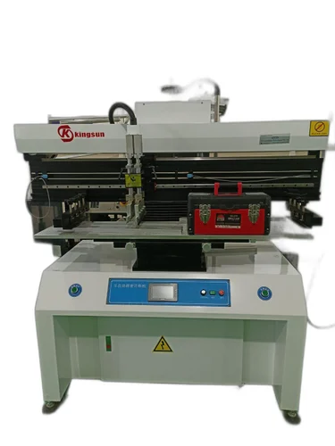
Technical parameter: Model 1200 Printing area 1250×320mm Fixed printing position PCB Outer Or Pin Positioning Table trimming Front/Back±
ProntoTEST-FIXTURE used by electronics manufacturers will accurately setup your Automatic Test Equipment (ATE), Flying Probe and design your "bed of nails" test fixturing. In minutes Unisoft ProntoTEST-FIXTURE software translates CAD and Bill of Ma
Electronics Forum | Sun Jul 26 07:52:35 EDT 2020 | sync40
Hello to everyone, Have you ever experienced soldermask bubbles inmediately after printed the soldermask itself? (for screen printing method of LPISM). I am not talking here about blistering or any outgassing defects after exposing to high temperatu
Electronics Forum | Wed Aug 25 19:31:22 EDT 1999 | Dave F
| JUST WANDERING IF ANYONE IS PRINTING ADHESIVE ON THE BOTTOM SIDE OF BOARD WITH THROUGH HOLE COMPONENTS ALREADY PLACED. I'VE BEEN TOLD IT IS POSSIBLE BUT WANT TO LOOK INTO THIS PROCESS IN DEPTH. | Chad: You don't need to YELL!!! Anyhow, yes we ha
Used SMT Equipment | Screen Printers
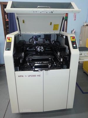
2002 Speedline UP 2000 Hi E Screen Printer Refurbished by OEM in 2006 Serial: 21223 Features: Cognex 5000; 4 Axis Motion Control; Tactile Sensor; Pass Through Conveyor; 2D Post Print Inspection; Y Snuggers; Vacuum Stencil Wiper;
Used SMT Equipment | Screen Printers
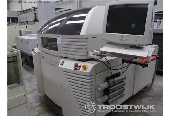
MPM-COOKSON, Serigraphic printing machine, type SPEEDLINE ULTRAPRINT 3000 - UP 3000/A, s.n. UO826/RF, with contrast support pins, online automatic frame cleaning (paper and solvent), double center camera 2D ( fiducial control 2D paste inspection), in
Industry News | 2003-06-26 09:02:38.0
The surface quality of printed circuit boards and components directly impacts performance and product life.
Industry News | 2003-04-18 08:31:57.0
Unichem to enhance its support and service for North American dry film photoresist and soldermask lamination equipment customers.
Parts & Supplies | Repair/Rework
PG-P6800 Main Features: 1、There are 3 independent heaters. The 1st and 2nd hot-air heaters can control multiple groups and segments temperature parameters. The 2nd heater can move up and down. The 3rd large area IR heater can preheat the PCB boar
Technical Library | 2016-11-30 15:53:15.0
The use of microvias in Printed Circuit Boards (PCBs) for military hardware is increasing as technology drives us toward smaller pitches and denser circuitry. Along with the changes in technology, the industry has changed and captive manufacturing lines are few and far between. As PCBs get more complicated, the testing we perform to verify the material was manufactured to our requirements before they are used in an assembly needs to be reviewed to ensure that it is sufficient for the technology and meets industry needs to better screen for long-term reliability. The Interconnect Stress Testing (IST) protocol currently used to identify manufacturing issues in plated through holes, blind, or buried vias are not necessarily sufficient to identify problems with microvias. There is a need to review the current IST protocol to determine if it is adequate for finding bad microvias or if there is a more reliable test that will screen out manufacturing inconsistencies. The objective of this research is to analyze a large population of PCB IST coupons to determine if there is a more effective IST test to find less reliable microvias in electrically passing PCB product and to screen for manufacturing deficiencies. The proposed IST test procedure will be supported with visual inspection of corresponding microvia cross sections and Printed Wiring Assembly (PWA) acceptance test results. The proposed screening will be shown to only slightly affect PCB yield while showing a large benefit to screening before PCBs are used in an assembly.
Technical Library | 2020-08-27 01:22:45.0
Initially adopted internal specifications for acceptance of printed circuit boards (PCBs) used for wire bonding was that there were no nodules or scratches allowed on the wirebond pads when inspected under 20X magnification. The nodules and scratches were not defined by measurable dimensions and were considered to be unacceptable if there was any sign of a visual blemish on wire-bondable features. Analysis of the yield at a PCB manufacturer monitored monthly for over two years indicated that the target yield could not be achieved, and the main reasons for yield loss were due to nodules and scratches on the wirebonding pads. The PCB manufacturer attempted to eliminate nodules and scratches. First, a light-scrubbing step was added after electroless copper plating to remove any co-deposited fine particles that acted as a seed for nodules at the time of copper plating. Then, the electrolytic copper plating tank was emptied, fully cleaned, and filtered to eliminate the possibility of co-deposited particles in the electroplating process. Both actions greatly reduced the density of the nodules but did not fully eliminate them. Even though there was only one nodule on any wire-bonding pad, the board was still considered a reject. To reduce scratches on wirebonding pads, the PCB manufacturer utilized foam trays after routing the boards so that they did not make direct contact with other boards. This action significantly reduced the scratches on wire-bonding pads, even though some isolated scratches still appeared from time to time, which caused the boards to be rejected. Even with these significant improvements, the target yield remained unachievable. Another approach was then taken to consider if wire bonding could be successfully performed over nodules and scratches and if there was a dimensional threshold where wire bonding could be successful. A gold ball bonding process called either stand-off-stitch bonding (SSB) or ball-stitch-on-ball bonding (BSOB) was used to determine the effects of nodules and scratches on wire bonds. The dimension of nodules, including height, and the size of scratches, including width, were measured before wire bonding. Wire bonding was then performed directly on various sizes of nodules and scratches on the bonding pad, and the evaluation of wire bonds was conducted using wire pull tests before and after reliability testing. Based on the results of the wire-bonding evaluation, the internal specification for nodules and scratches for wirebondable PCBs was modified to allow nodules and scratches with a certain height and a width limitation compared to initially adopted internal specifications of no nodules and no scratches. Such an approach resulted in improved yield at the PCB manufacturer.

www.unisoft-cim.com/pcbtest.htm - In minutes the Unisoft ProntoTEST-FIXTURE software translates CAD & BOM files into real reference designators, netlists, X/Y component pin geometries, values, tolerances, part numbers, etc. This data is used by Test
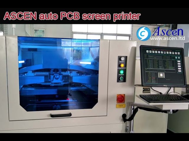
https://www.ascen.ltd/Products/Solder_paste_printer/513.html full auto PCB screen printer and SMT solder paste printing machine with Image and optical system,It is a very accurate fully automatic SMT stencil printer.automatic PCB screen printer main
Training Courses | | | Cable and Wire Harness Assembly Training Courses
Browse training and certification programs for wire harness cable and connector assembly.
Training Courses | | | Cable and Wire Harness Assembly Training Courses
Browse training and certification programs for wire harness cable and connector assembly.
Events Calendar | Mon Aug 10 00:00:00 EDT 2020 - Mon Aug 10 00:00:00 EDT 2020 | ,
Monitoring & Bench marking Your Processes and Assembly Yields
Events Calendar | Mon Mar 18 00:00:00 EDT 2019 - Mon Mar 18 00:00:00 EDT 2019 | ,
Webinar: Stencil Design for Solder Paste, In Process Inspection & Process Defects
Career Center | Newburyport, Massachusetts USA | Sales/Marketing
Needed: Experienced Sales Persons for Central and Western United States based in Chicago and Southern California. Responsible for sales of all products for SMT placement, screen printing, screen cleaners and inspection devices. Please forward resume
Career Center | North Attleboro, Massachusetts USA | Production
Operate Mydata equipment able to read bom and assembly drawings inspect pcb screen printing training is available for anyone interested.
Career Center | , | Engineering,Maintenance,Technical Support
Dear Sir/Madam, I am having the 10 years exprience in SMT field. Currently I am working in Service industry as Senior Engineer. Specially I am exprience and trained in FUJI and Speedline machines. Earlier I worked with Manufacturing Industry.
Career Center | Delhi, India | Maintenance,Production,Sales/Marketing,Technical Support
7 Years of experiance in SMT line
| https://www.feedersupplier.com/sale-13005432-dek-horizon-03ix-smt-stencil-printer-screen-printing-machine.html
: DEK Horizon 03iX Smt Stencil Printer Screen Printing Machine Lead Time: 5 Days After Payment Condition: Original Used Application
KingFei SMT Tech | http://www.smtspare-parts.com/sale-8463718-dek-screen-printing-machine-parts-191088-original-new-solvent-pump-assy.html
DEK Screen Printing Machine Parts 191088 Original New Solvent Pump Assy Leave a Message We will call you back soon! Your message must be between 20-3,000 characters
Our Company handle AOI (Auto Optical Inspection) and SPI (Solder Paste Inspection) Machines.
Equipment Dealer / Broker / Auctions
Hwaseong-si, Gyeonggi-do, Korea
Hwaseong-si, South Korea
Phone: +82-1029254936
winsouce.jpg)


