Industry News | 2019-08-21 16:55:59.0
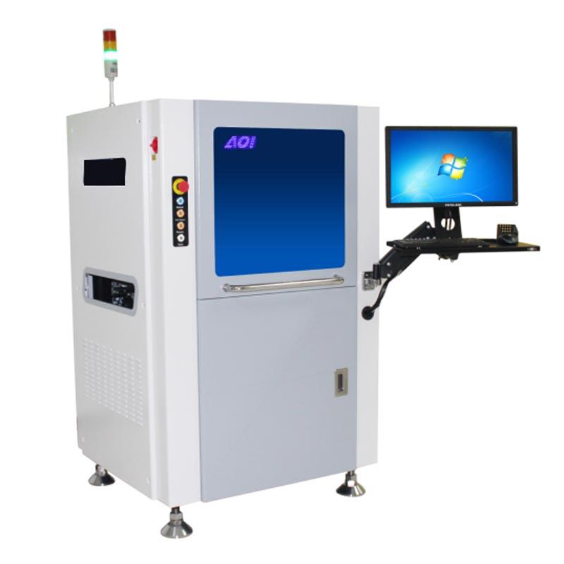
MIRTEC will exhibit in Booth #305 at SMTA International. MIRTEC will showcase the latest advancements in their award-winning 3D AOI and SPI Systems at the two-day event.
Industry News | 2020-06-30 15:07:32.0
MIRTEC is excited to announce its participation in an exclusive ONLINE CONFERENCE & EXPO. The event will be broadcast live on Wednesday, July 8, 2020 from 10 a.m. - 2:30 p.m. EST and will include a full program of live presentations, interviews and special guests.
Industry News | 2017-04-27 17:50:10.0
In response to mounting concern about the shortage of U.S. workers with skills needed by electronics manufacturers, IPC – Association Connecting Electronics Industries® conducted a “fast-facts” study to learn more about the skills gap as it affects U.S. electronics assembly manufacturers. The results, published last week within Findings on the Skills Gap in U.S. Electronics Manufacturing, indicate that most companies are having a hard time recruiting qualified production workers, and an even harder time finding qualified engineers and other technical professionals.
automated optical inspection AOI manufacturers in China keywords: AOI machine, AOI, automated optical inspection, AOI machine cost, AOI machine for PCB, SMT AOI machine, SMT AOI, SMD AOI, SMD AOI machine CATEGORY ITEM
Technical Library | 2008-03-18 12:36:31.0
This paper examines the construction of a notebook mainboard with more than 2000 components and no wave soldering required. The board contains standard SMD, chipset BGAs, connectors, through hole components and odd forms placed using full automation and soldered after two reflow cycles under critical process parameters. However, state of the art technology does not help if the process parameters are not set carefully. Can all complex BGAs, THTs and even screws be soldered on a single stencil? What will help us overcome bridging, insufficient solder and thombstoning issues? This paper will demonstrate the placement of all odd shape components using pin-in-paste stencil design and full completion of the motherboard after two reflow cycles.
Industry News | 2019-11-05 22:08:21.0
Via in pad is the design practice of placing a via in the copper landing pad of a component. Compared to standard PCB via routing, via in pad allows a design to use smaller component pitch sizes and further reduce the PCBs overall size. With component manufactures pushing smaller parts every year and the demand from consumers for smaller devices, the usage of via in pad practices by hardware engineers have become more commonplace. In this article, we will discuss the differences between via in pad and traditional vias, when should you use via in pad, and how to design for it.
500,000 components per hour Maximum Board Size: 22” x 20” (560mm x 510mm) Clearance: 2” (50mm) top and bottom Minimum Component Size: 0201; 01005 with high magnification option
Technical Library | 2023-11-20 18:10:20.0
The electronics production is prone to a multitude of possible failures along the production process. Therefore, the manufacturing process of surface-mounted electronics devices (SMD) includes visual quality inspection processes for defect detection. The detection of certain error patterns like solder voids and head in pillow defects require radioscopic inspection. These high-end inspection machines, like the X-ray inspection, rely on static checking routines, programmed manually by the expert user of the machine, to verify the quality. The utilization of the implicit knowledge of domain expert(s), based on soldering guidelines, allows the evaluation of the quality. The distinctive dependence on the individual qualification significantly influences false call rates of the inbuilt computer vision routines. In this contribution, we present a novel framework for the automatic solder joint classification based on Convolutional Neural Networks (CNN), flexibly reclassifying insufficient X-ray inspection results. We utilize existing deep learning network architectures for a region of interest detection on 2D grayscale images. The comparison with product-related meta-data ensures the presence of relevant areas and results in a subsequent classification based on a CNN. Subsequent data augmentation ensures sufficient input features. The results indicate a significant reduction of the false call rate compared to commercial X-ray machines, combined with reduced product-related optimization iterations.
Industry News | 2017-01-18 05:21:35.0
This photo CD ROM provides the process or quality engineer with a source of PIHR photographs of the assembly process, components and process defects which may be used in company inspection document or training presentations. They may be simply pasted into any document for in house company use. Now over 250 photographs are provided in either jpg or tif file format for use in PowerPoint, Word inspection standards or online publications royalty free http://www.bobwillis.co.uk/product-category/photo-cd-rom/
Industry News | 2015-09-16 10:43:38.0
Inovar announces that it recently purchased and installed four MS-11 solder paste inspection (SPI) systems from MIRTEC.


