Industry Directory | Distributor / Manufacturer
AOI Vision is the specialized supplier of advanced materials and engineering solutions for SMT PCB screen printing industry. We team up with industry leaders who are equipped with cutting edge technology and innovative products.
3550 sq. mm second (> 5.5 sq. in / second) Maximum Board Size: 350mm x 250mm (14 x 10 in.) Minimum Board Size: 50mm x 50mm (2 x 2 in.) Topside Clearance: 25mm (1 in.) Bot
3550 sq. mm second (> 5.5 sq. in / second) Maximum Board Size: 350mm x 250mm (14 x 10 in.) Minimum Board Size: 50mm x 50mm (2 x 2 in.) Topside Clearance: 25mm (1 in.) Bot
Technical Library | 2014-06-05 16:44:07.0
Stencil printing capability is becoming more important as the range of component sizes assembled on a single board increases. Coupled with increased component density, solder paste sticking to the aperture sidewalls and bottom of the stencil can cause insufficient solder paste deposits and solder bridging. Yield improvement requires increased focus on stencil technology, printer capability, solder paste functionality and understencil cleaning.(...) The purpose of this research is to study the wipe sequence, wipe frequency and wipe solvent(s) and how these factors interact to provide solder paste printing yield improvement.
Industry News | 2016-03-11 00:15:11.0
SHENMAO Solder Preforms offer accurate solder deposition for various soldering processes. Reel packaged Solder Preforms provide opportunity for automation and efficient application to supplement solder when insufficient quantity solder paste is provided by design.
Technical Library | 2023-05-22 16:49:42.0
Our customers' issues • Apertures are getting smaller • Paste does not release as well • Contaminates the bottom of the stencil • Increases defects / reduces yield Insufficient solder Bridging Solder balls on surface of PCB Flux residue • Requires more frequent cleaning • Reduced efficiency (wasted time) • Increased use of consumables (cost) USC fabric (use "cheap" fabric to reduce cost) Lint creates more defects Cleaning chemistries (use IPA to reduce cost) IPA breaks down flux and can create more defects
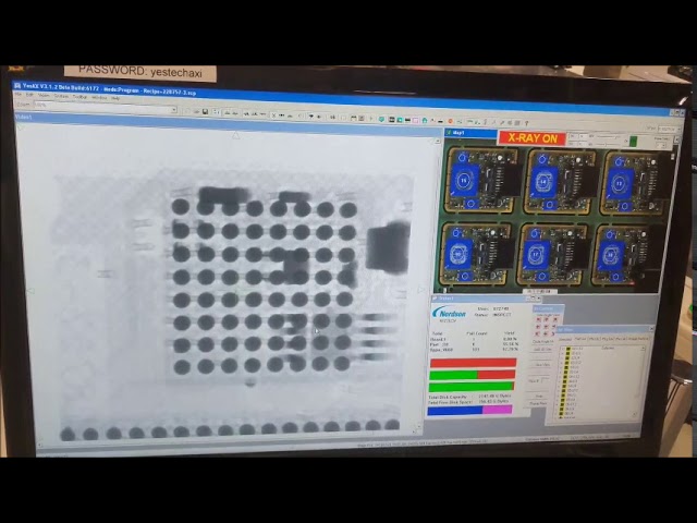
This is a demonstration of the YESTech YTX-X3 3D X-Ray inspecting pcbs in production. This YTX-X3 is available at the Capital Equipment Exchange. https://www.ce-exchange.com/details/?product=7426&pn=YESTech-YTX-X3-3D-X-Ray
SUPERIOR VISION 4000 � SUPERIOR SOLDER DEFECT DETECTION The Photon Dynamics Superior Vision (SV) 4000 AOI system delivers comprehensive defect detection. Designed for high-pulse production of large-format, high-density and small component PWAs, t
SUPERIOR VISION 6000 � UNRIVALED SOLDER DEFECT DETECTION The Photon Dynamics Superior Vision (SV) 6000 AOI system delivers comprehensive defect detection. Designed for high-pulse production of large-format, high-density and small component PWAs,
Technical Library | 2013-07-25 14:02:15.0
Bottom-termination components (BTC), such as QFNs, are becoming more common in PCB assemblies. These components are characterized by hidden solder joints. How are defects on hidden DFN joints detected? Certainly, insufficient solder joints on BTCs cannot be detected by manual visual inspection. Nor can this type of defect be detected by automated optical inspection; the joint is hidden by the component body. Defects such as insufficients are often referred to as "marginal" defects because there is likely enough solder present to make contact between the termination on the bottom-side of the component and the board pad for the component to pass in-circuit and functional test. Should the board be subjected to shock or vibration, however, there is a good chance this solder connection will fracture, leading to an open connection.


