Technical Library | 2016-11-30 21:30:50.0
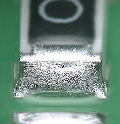
Mid-chip solder balling is a defect typically associated with solder paste exhibiting poor hot slump and/or insufficient wetting during the reflow soldering process, resulting in paste flowing under the component or onto the solder resist. Once molten, this solder is compressed and forced to the side of the component, causing mid-chip solder balling.This paper documents the experimental work performed to further understand the impact on mid-chip solder balling from both the manufacturing process and the flux chemistry.
Technical Library | 2016-10-03 08:28:47.0
With the miniaturization of electronic device, Land Grid Array (LGA) or QFN has been widely used in consumer electronic products. However there is only 20-30 microns gap left between LGA and the substrate, it is very difficult for capillary underfill to flow into the large LGA component at room temperature. Insufficient underfilling will lead to the loss of quality control and the poor reliability issue. In order to resolve these issues, a room temperature fast flow reworkable underfill has been successfully developed with excellent flowability. The underfill can flow into 20 microns gap and complete the flow of 15mm distance for about 30 seconds at room temperature. The curing behavior, storage, thermal cycling performance and reworkability will be discussed in details in this paper.
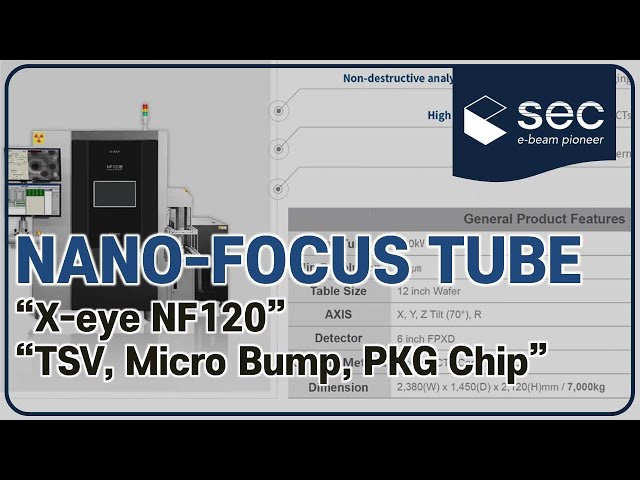
#Xray#Inspection#SEC Nano-focus Tube of 200 nano resolution which is specialized for sub-micron defects of Semiconductor Packaging, Wafer Level Packaging(WLP). -Non-destructive Analysis System -High-Resolution Image with Dual Type CTs -Application

High Value Stencil Screen Printing Solutions from JUKI. The PMAXII printers utilize a patented mathematical calculating algorithm to ensure the machine's high accuracy print alignment that easily achieves 01005 (0402 metric) printing. Vision
Industry News | 2020-06-07 04:44:33.0
PDR X-ray Solutions is pleased to announce that its 2D and 2D+ X-ray systems have set a new industry standard for high-quality X-ray images at an affordable price. Choosing the correct system for your requirements such as X-ray for quality control or X-ray for process control is vital for the success of both X-ray circuit board inspection programs as well as X-ray semiconductor inspection programs.
Technical Library | 2018-05-23 12:12:43.0
Driven by miniaturization, cost reduction and tighter requirements for electrical and thermal performance, the use of lead-frame based bottom-termination components (LF-BTC) as small-outline no-leads (SON), quad-flat no leads (QFN) packages etc., is increasing. However, a major distractor for the use of such packages in high-reliability applications has been the lack of a visible solder (toe) fillet on the edge surface of the pins: because the post-package assembly singulation process typically leaves bare copper leadframe at the singulation edge, which is not protected against oxidation and thus does not easily solder-wet, a solder fillet (toe fillet) does not generally develop.

ITW EAE MPM Edison Printing System
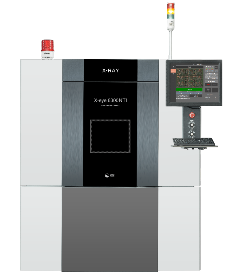
In-Line X-ray Inspection System Automatically in-line inspect Solder joint defects of PCBA and other defects on Hidden Components. Able to judge Good/NG fast with inspection speed of 1sec/FOV and the program can set ROIs conveniently. Performing X-r
New Equipment | Solder Materials
AIM introduces M8 Solder Paste, a high reliability no clean paste for use with SAC305, REL22, REL61, and Sn/Pb alloys. M8 no clean solder paste is designed for the most demanding high density electronic assemblies. An evolution of the highly success
Industry News | 2010-04-28 20:24:38.0
NASHVILLE — Kyzen, a world leading provider of environmentally responsible precision cleaning products for electronics and high-technology manufacturing operations, announces that Rich Brooks held a successful presentation at the SMTA Silicon Valley Chapter meeting, which took place on Thursday, April 22, 2010 from 3-5:30 p.m. at EET, Inc. in Reno, NV.


winsouce.jpg)
