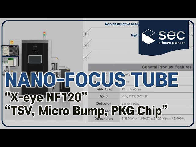
#Xray#Inspection#SEC Nano-focus Tube of 200 nano resolution which is specialized for sub-micron defects of Semiconductor Packaging, Wafer Level Packaging(WLP). -Non-destructive Analysis System -High-Resolution Image with Dual Type CTs -Application

High Value Stencil Screen Printing Solutions from JUKI. The PMAXII printers utilize a patented mathematical calculating algorithm to ensure the machine's high accuracy print alignment that easily achieves 01005 (0402 metric) printing. Vision
Industry News | 2020-06-07 04:44:33.0
PDR X-ray Solutions is pleased to announce that its 2D and 2D+ X-ray systems have set a new industry standard for high-quality X-ray images at an affordable price. Choosing the correct system for your requirements such as X-ray for quality control or X-ray for process control is vital for the success of both X-ray circuit board inspection programs as well as X-ray semiconductor inspection programs.
Technical Library | 2018-05-23 12:12:43.0
Driven by miniaturization, cost reduction and tighter requirements for electrical and thermal performance, the use of lead-frame based bottom-termination components (LF-BTC) as small-outline no-leads (SON), quad-flat no leads (QFN) packages etc., is increasing. However, a major distractor for the use of such packages in high-reliability applications has been the lack of a visible solder (toe) fillet on the edge surface of the pins: because the post-package assembly singulation process typically leaves bare copper leadframe at the singulation edge, which is not protected against oxidation and thus does not easily solder-wet, a solder fillet (toe fillet) does not generally develop.
In-Line X-ray Inspection System Automatically in-line inspect Solder joint defects of PCBA and other defects on Hidden Components. Able to judge Good/NG fast with inspection speed of 1sec/FOV and the program can set ROIs conveniently. Performing X-r

ITW EAE MPM Edison Printing System
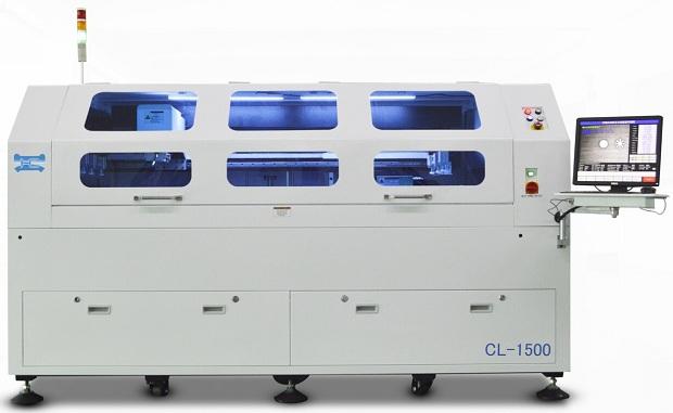
CL-1500 high precision automatic solder paste screen printer designed for high precision screen printing or stencil printing for PCBS of LED Lighting products. Support PCB size from 100mm x 50mm to 1500mm x 350mm and PCB thickness from 0.8mm to
Industry News | 2019-08-15 07:31:59.0
AXI is short for automated X-ray inspection, it's one of the most commonly used approaches for defect inspection in PCB Assembly.
New Equipment | Solder Materials
Indium Corporation manufactures high quality solder powders and pastes. Powders are available in hundreds of alloys and a full range of sizes. Solder pastes can be made from these powders using a wide variety of flux vehicles to get the best fit for
Industry News | 2010-04-28 20:24:38.0
NASHVILLE — Kyzen, a world leading provider of environmentally responsible precision cleaning products for electronics and high-technology manufacturing operations, announces that Rich Brooks held a successful presentation at the SMTA Silicon Valley Chapter meeting, which took place on Thursday, April 22, 2010 from 3-5:30 p.m. at EET, Inc. in Reno, NV.


.gif)


