New Equipment | Board Handling - Storage
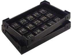
Dissipative Surface Stackable Eliminates Bags Durable Recyclable CorStacker Trays are made of durable Corstat™ shielding corrugated. The construction is double wall with injection molded corner stackers attached for secure stacking. The tray
Industry Directory | Manufacturer / Other
Simplimatic Automation designs and manufacturers complete material handling systems for circuit board, Auer boat, JEDEC tray processes, including product marking. Full line of pallet, part, and puck handling equipment. Global on-site support.

Intrinsic Quality is pleased to offer a variety of Test Fixture Development Services that include fixture building, tester interface building, harness building, troubleshooting, maintenance, design, and engineering. IQ’s fixtures are built to exactin
Industry Directory | Distributor
Representing Foreign Principals for their range of SMT / PCB Assembly equipments.
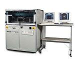
Similar to D-9000, featuring a larger scanning area (24" x 24"). Ideally suited for large printed circuit boards and multiple tray analyses.
Industry Directory | Manufacturer
Development and manufacturing of X-ray based inspection systems.
Industry Directory | Manufacturer
The Future of Electronics is here - With Squink at your Desktop, print and assemble PCBs in minutes instead of weeks for less than a cup of coffee. Go from CAD design to PCB without the pain and cost.
Parts & Supplies | Assembly Accessories
BOLT N510017510AA SSS 003 Hexagon socket button head screw M3X4-10.9 A2J (Trivalent) BOLT N510017372AA Hexagon socket head cap screw M4X5-10.9 A2J (Trivalent) Tray Feeder Wiring:NPM N610070389AD EL16CC_PbF: Sensor Relay Board: LED KXFE0019A00
Technical Library | 2020-08-27 01:22:45.0
Initially adopted internal specifications for acceptance of printed circuit boards (PCBs) used for wire bonding was that there were no nodules or scratches allowed on the wirebond pads when inspected under 20X magnification. The nodules and scratches were not defined by measurable dimensions and were considered to be unacceptable if there was any sign of a visual blemish on wire-bondable features. Analysis of the yield at a PCB manufacturer monitored monthly for over two years indicated that the target yield could not be achieved, and the main reasons for yield loss were due to nodules and scratches on the wirebonding pads. The PCB manufacturer attempted to eliminate nodules and scratches. First, a light-scrubbing step was added after electroless copper plating to remove any co-deposited fine particles that acted as a seed for nodules at the time of copper plating. Then, the electrolytic copper plating tank was emptied, fully cleaned, and filtered to eliminate the possibility of co-deposited particles in the electroplating process. Both actions greatly reduced the density of the nodules but did not fully eliminate them. Even though there was only one nodule on any wire-bonding pad, the board was still considered a reject. To reduce scratches on wirebonding pads, the PCB manufacturer utilized foam trays after routing the boards so that they did not make direct contact with other boards. This action significantly reduced the scratches on wire-bonding pads, even though some isolated scratches still appeared from time to time, which caused the boards to be rejected. Even with these significant improvements, the target yield remained unachievable. Another approach was then taken to consider if wire bonding could be successfully performed over nodules and scratches and if there was a dimensional threshold where wire bonding could be successful. A gold ball bonding process called either stand-off-stitch bonding (SSB) or ball-stitch-on-ball bonding (BSOB) was used to determine the effects of nodules and scratches on wire bonds. The dimension of nodules, including height, and the size of scratches, including width, were measured before wire bonding. Wire bonding was then performed directly on various sizes of nodules and scratches on the bonding pad, and the evaluation of wire bonds was conducted using wire pull tests before and after reliability testing. Based on the results of the wire-bonding evaluation, the internal specification for nodules and scratches for wirebondable PCBs was modified to allow nodules and scratches with a certain height and a width limitation compared to initially adopted internal specifications of no nodules and no scratches. Such an approach resulted in improved yield at the PCB manufacturer.
.jpg)
Parts & Supplies | Pick and Place/Feeders
Hot sell JUKI 750 760 OCC LIGHT CIRCUIT BOARD A ASM E86127250A0 Original new and used Supply all juki spare parts at low price JUKI 40049291 TRAY UNIT www.fujintai.com JUKI 40049292 OP BOX UNIT 6S FUJINTAI TECHNOLOGY CO.,LTD JUKI 40049308 OP

Midwest Circuit Technology provides Carbide Router Bits and End Milling Cuters for use in PCB Depaneling equipment. We have over 35 years of supplying tools and machining experience in drilling, Routing, Test Fixture manufacture.
114 Barrington Town Square
Aurora, OH USA
Phone: 13309956900


