Lite Fast SR-1000, a UV Solder Mask, was designed to screen print over conductive traces, landing pads, resistors, fuses and capacitors on Printed Circuit Boards (PCBs) and ceramic substrates. Other applications include metal and various plastics.
.jpg)
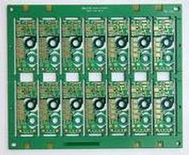
Layer Count: 8L Board Thickness: 1.0mm Panel Dimension:190*86mm/2up Material: S1141 Copper on board surface: 35μm Min Hole Diameter: 0.1mm Min line Width/Space: 8/8mil Surface Finish: ENIG+Selective OSP in BGA area This quick turn PCB is manufacture
Circuit Technology Center, Inc.
Industry Directory | Manufacturer
Caring Circuit specialises in the supply of prototype, small and medium-series PCBs factory in Shenzhen,China.We are a leading provider of custom Single layer,double layer,multilayer rigid PCBs.
Technical Library | 2015-08-13 15:52:40.0
Pad cratering has become more prevalent with the switch to lead free solders and lead free compatible laminates. This mainly is due to the use of higher reflow temperature, stiffer Pb-free solder alloys, and the more brittle Pb-free compatible laminates. However, pad cratering is difficult to detect by monitoring electric resistance since pad cratering initiates before an electrical failure occurs. Several methods have been developed to evaluate laminate materials' resistance to pad cratering. Pad-solder level tests include ball shear, ball pull and pin pull. The detailed methods for ball shear, ball pull, and pin pull testing are documented in an industry standard IPC-9708. Bansal, et al. proposed to use acoustic emission (AE) sensors to detect pad cratering during four-point bend test. Currently there is an industry-working group working on test guidelines for acoustic emission measurement during mechanical testing.
Events Calendar | Tue Jan 23 00:00:00 EST 2018 - Tue Jan 23 00:00:00 EST 2018 | New Milford, Connecticut USA
FREE Webinar: Eliminate Circuit Board Problems and Failure Modes

SIPAD Systems Incorporated (SSi) is the Exclusive Supplier of SIPAD solid solder deposit in North America and the only SIPAD Solid Solder Deposit (SSD) coating service bureau in the world. SIPAD Systems Inc. supplies SIPAD solid solder coating servi
New Equipment | Test Equipment
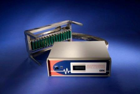
Auto-SIR – Performs Surface Insulation Resistance testing in accordance with all major international standards: IEC 61189-5, ISO 9455-17, IPC-TM-650, BELCORE GR-78-CORE, DIN German & JIS Japanese standards. Includes elements of ANSI/IPC-JSTD001C (as
Parts & Supplies | Circuit Board Assembly Products
PULANG TECHNOLOGY CO,.LTDOffers electronic manufacturing services including PCB designing, electronic contract manufacturing including electronic product design, electronic product development, electronic product repair, PCB manufacturing, electronic
Technical Library | 2012-10-18 21:58:51.0
First published in the 2012 IPC APEX EXPO technical conference proceedings. In this paper, we report on a comprehensive study regarding the morphology evolution and voiding of SnAgCu solder joints on the central pad of two different packages – QFN and an Agilent package called TOPS – on PCBs with a Ni/Au surface finish.
IPC is the trade association for the printed wiring board and electronics assembly industries.
Training Provider / Events Organizer / Association / Non-Profit
3000 Lakeside Drive, 309 S
Bannockburn, IL USA
Phone: 847-615-7100


