Industry News | 2003-09-11 16:50:12.0
The printed circuit board industry is an ever-changing marketplace. The technologies of today certainly aren�t standing still, and neither should today�s PCB designer
Industry Directory | Manufacturer
Hi-Rel Thick Film Substrates, Multilayer, Thru-Hole/Edge Around, 2mil Lines Etched Conductors
Used SMT Equipment | Soldering - Reflow
Electrovert Omniflo 10 E GREAT MACHINE-great deal! Condition: Very Good-working 2001 Model Edge Rail Conveyor (no mesh) 10 Heat zones, 4 cooling zones, Left to Right flow Clean and complete-Photos available Price $7,900.00 Clean and comple
Industry Directory | Manufacturer
Services, components and consumables for electronic manufacturing
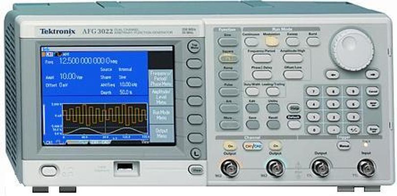
Used SMT Equipment | General Purpose Test & Measurement
Arbitrary Function Generator. Unmatched performance, versatility, intuitive operation and affordability make the AFG3000 Series of Function, Arbitrary Waveform and Pulse Generators the most useful instruments in the industry. Users can choose from 12
Fine Line Stencil offers various frame systems depending on what your unique printing process requires. VectorGuard® SMT Stencil Technology. VectorGuard® is a patented frameless stencil tensioning system offerin
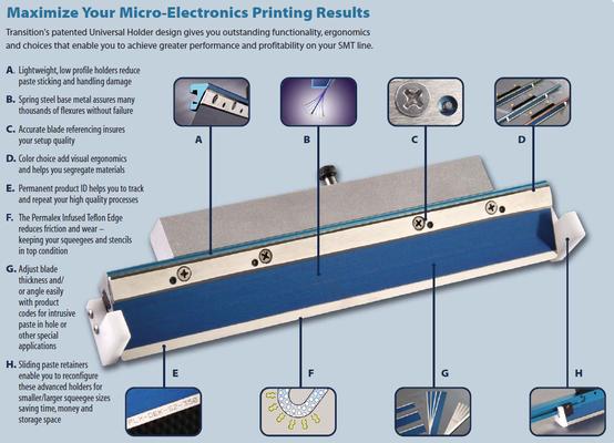
Maximize Your Micro-Electronics Printing Results Transition's patented Universal Holder design gives you outstanding functionality, ergonomics and choices that enable you to achieve greater performance and profitability on your SMT line. Permalex E
Technical Library | 2010-05-06 18:46:29.0
Stencil printing technology has come a long way since the early 80’s when SMT process gained importance in the electronics packaging industry. In those early days, components were fairly large, making the board design and printing process relatively simple. The current trend in product miniaturization has led to smaller and more complex board designs. This has resulted into designs with maximum area utilization of the board space. It is not uncommon, especially for hand held devices, to find components only a few millimeters from the edge of the board. The board clamping systems used in the printing process have become a significant area of concern based on the current board design trend.
Technical Library | 2018-04-05 10:40:43.0
The miniaturization of microchips is always driving force for revolution and innovation in the electronic industry. When the pitch of bumps is getting smaller and smaller the ball size has to be gradually reduced. However, the reliability of smaller ball size is getting weaker and weaker, so some traditional methods such as capillary underfilling, corner bonding and edge bonding process have been being implemented in board level assembly process to enhance drop and thermal cycling performance. These traditional processes have been increasingly considered to be bottleneck for further miniaturization because the completion of these processes demands more space. So the interest of eliminating these processes has been increased. To meet this demand, YINCAE has developed solder joint encapsulant adhesives for ball bumping applications to enhance solder joint strength resulting in improving drop and thermal cycling performance to eliminate underfilling, edge bonding or corner bonding process in the board level assembly process. In this paper we will discuss the ball bumping process, the reliability such as strength of solder joints, drop test performance and thermal cycling performance.
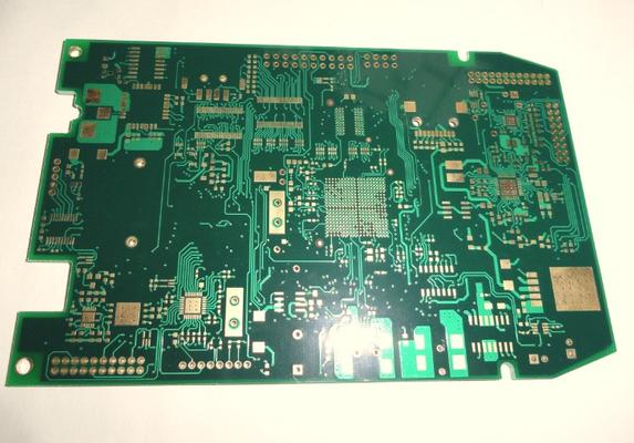
Layer: 8 layers Material: FR-4 Board Thickness: 0.6mm Surface Finish: Immersion Gold 1~4u Copper Thickness: 1/3 oz Impedance, 4/4mils width/spacing Layers: 2--36layers Max manufacturing size: 640mm*1100mm Copper foil thickness: 0.5OZ-13OZ M


