New Equipment | Design Services
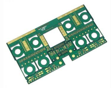
Layer:4 Material:FR-4 4/4/4/4oz Thickness:2.0 Minimum hole:0.35mm Minimum Tracc/Spacing:12mil/15mil Application:power supply Layers: 2--36layers Max manufacturing size: 640mm*1100mm Copper foil thickness: 0.5OZ-13OZ Min line width/space:
Industry Directory | Manufacturer
Speedy Circuits manufactures technically demanding PCBs, flex & rigid-flex circuits, metal core boar
Industry Directory | Consultant / Service Provider / Manufacturer
EIIT is an engineering company with 27 years experience in the design & manufacture of test equipment: off-line and In-line ICT, ISP, FCT, BS. Screening and BurnIn Testers and Modular Assembly Systems
Industry Directory | Distributor / Manufacturer
Venture Mfg. Co. is one of the most trusted and credible names in the industry for manufacturing Linear Actuators & Linear motion control products of supreme quality.
Used SMT Equipment | In-Circuit Testers
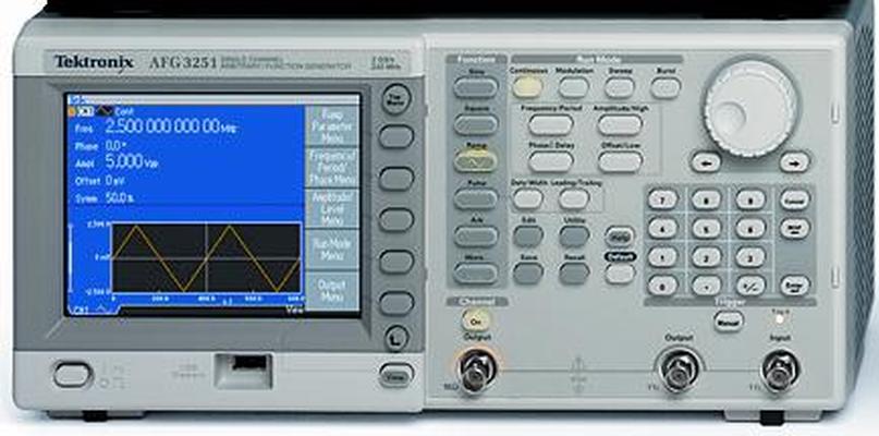
Tektronix AFG3251 Abitrary Function Generator. Unmatched performance, versatility, intuitive operation and affordability make the AFG3000 Series of Function, Arbitrary Waveform and Pulse Generators the most useful instruments in the industry. Use
New Equipment | Solder Paste Stencils
Tropical Stencil’s Laser Cut SMT Stencils are produced utilizing high speed lasers to produce the smoothest aperture wall possible. Far superior to chemically etched stencils, and with emerging new materials, stencils are produced using “fine grain”

New Equipment | Fabrication Services
PentaLogix offers three PCB fabrication services: US QuickTurn Prototype PCB Includes full Smart DFM design check US made high-quality circuit boards FAST turn times: 2-layer in 1-2 days, 4-6 layer in 2-4 days Tin lead HASL or OSP RoH

Layer: 2 Material: FR-4 Board Thickness: 1.6mm Surface Finish: HAL Copper Thickness: 2/2 oz Green Solder Mask Layers: 2--36layers Max manufacturing size: 640mm*1100mm Copper foil thickness: 0.5OZ-13OZ Min line width/space: 3mil/3mil Min
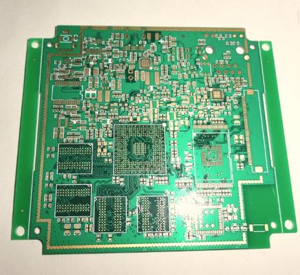
Layer: 6 layers Material: FR-4 Board Thickness: 1.0mm Surface Finish:ENIG Copper Thickness: 1 oz all layers Blind via L1~L2 and L1~L3 Layers: 2--36layers Max manufacturing size: 640mm*1100mm Copper foil thickness: 0.5OZ-13OZ Min line width
Technical Library | 2015-05-28 17:34:48.0
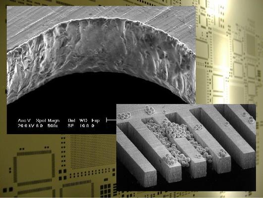
The printed circuit board assembly industry has long embraced the "Smaller, Lighter, Faster" mantra for electronic devices, especially in our ubiquitous mobile devices. As manufacturers increase smart phone functionality and capability, designers must adopt smaller components to facilitate high-density packaging. Measuring over 40% smaller than today's 0402M (0.4mmx0.2mm) microchip, the new 03015M (0.3mm×0.15mm) microchip epitomizes the bleeding-edge of surface mount component miniaturization. This presentation will explore board and component trends, and then delve into three critical areas for successful 03015M adoption: placement equipment, assembly materials, and process controls. Beyond machine requirements, the importance of taping specifications, component shape, solder fillet, spacing gap, and stencil design are explored. We will also examine how Adaptive Process Control can increase production yields and reduce defects by placing components to solder position rather than pad. Understanding the process considerations for 03015M component mounting today will help designers and manufacturers transition to successful placement tomorrow.


