Up to 20 layers, 4 mil traces / spaces, 6 mil drilled holes and Book-bind capability. MIL-P-50884 approved for adhesiveless materials. Deliveries down to 3 days are available.
Capabilities include: Up to 30 layers, 3 mil traces and spaces, 6 mil drilled holes, available in 24 hours to 2 weeks.
Capabilities include: 1 to 20 layers, adhesive based or adhesiveless, 3 mil traces and spaces, 6 mil drilled holes, available in 3 days to 20 days
Capabilities include: 2 to 20 layers, 3 mil traces and spaces, 6 mil bond pitch, 6 mil drilled holes, internal cavity and consistent wire bondable gold.
min trace width/space 3 mils, min hole diameter 0.15mm

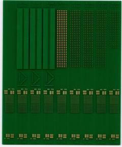
Layer: 12 Material: FR4(Tg170) Board thickness: 1.6mm Min trace width/spacing: 4/4mil Min hole size: 0.2mm Impedance control
Technical Library | 2021-06-21 19:34:02.0
In this era of electronics miniaturization, high yield and low-cost integrated circuit (IC) substrates play a crucial role by providing a reliable method of high density interconnection of chip to board. In order to maximize substrate real-estate, the distance between Cu traces also known as line and space (L/S) should be minimized. Typical PCB technology consists of L/S larger than 40 µ whereas more advanced wafer level technology currently sits at or around 2 µm L/S. In the past decade, the chip size has decreased significantly along with the L/S on the substrate. The decreasing chip scales and smaller L/S distances has created unique challenges for both printed circuit board (PCB) industry and the semiconductor industry. Fan-out panel-level packaging (FOPLP) is a new manufacturing technology that seeks to bring the PCB world and IC/semiconductor world even closer. While FOPLP is still an emerging technology, the amount of high-volume production in this market space provide a financial incentive to develop innovative solutions in order to enable its ramp up. The most important performance aspect of the fine line plating in this market space is plating uniformity or planarity. Plating uniformity, trace/via top planarity, which measures how flat the top of the traces and vias are a few major features. This is especially important in multilayer processing, as nonuniformity on a lower layer can be transferred to successive layers, disrupting the device design with catastrophic consequences such as short circuits. Additionally, a non-planar surface could also result in signal transmission loss by distortion of the connecting points, like vias and traces. Therefore, plating solutions that provide a uniform, planar profile without any special post treatment are quite desirable.
Technical Library | 2018-10-18 15:41:45.0
One specific market space of interest to emerging printed electronics is In Mold Label (IML) technology. IML is used in many consumer products and white good applications. When combined with electronics, the In Mold Electronics (IME) adds compelling new product functionality. Many of these products have multi-dimensional features and therefore require thermoforming processes in order to prepare the labels before they are in-molded. While thermoforming is not a novel technique for IML, the addition of printed electronic functional traces is not well documented. There is little or no published work on printed circuit performance and design interactions in the thermoforming process that could inform improved IME product designs. A general full factorial Design of Experiments (DOE) was used to analyze the electrical performance of the conductive silver ink trace/polycarbonate substrate system. Variables of interest include trace width, height of draw, and radii of both top and bottom curvatures in the draw area. Thermoforming tooling inserts were fabricated for eight treatment combinations of these variables. Each sample has one control and two formed strips. Electrical measurements were taken of the printed traces on the polymer sheets pre- and post- forming with a custom fixture to evaluate the effect on resistance. The design parameters found to be significant were draw height and bottom radius, with increased draw and smaller bottom curvature radii both contributing to the circuits’ resistance degradation. Over the ranges evaluated, the top curvature radii had no effect on circuit resistance. Interactions were present, demonstrating that circuit and thermoforming design parameters need to be studied as a system. While significant insight impacting product development was captured further work will be executed to evaluate different ink and substrate material sets, process variables, and their role in IME.
Industry Directory | Consultant / Service Provider
Quick Turn PCBs, 5 Prototype PCBs at $25.00ea. Fast5Protos delivers quality PCBs in 1-2 days. Free tooling, test, & shipping.
Industry Directory | Manufacturer
Circuits, LLC is a quality-driven, customer-focused manufacturer of highly reliable built-to-spec flexible printed circuit boards serving the defense, industrial, and medical markets.


