High Tech, Quick Turn, Manufacturer of PCB's up to 44 layer count. Specializing in Prototype and R&D. Mil-Spec 31032 & 55110 Certified. Located in Fremont, CA & Amesbury, MA.
Industry Directory | Manufacturer
Professional, Reliable,High Quality,Low Cost, Rapid Delivery PCB manufacturer
Industry Directory | Manufacturer
We provide cost effective, custom printed circuit boards (PCBs) through an instant online system. We also provide PCB Assemb
Training Courses | | | IPC-7711/7721 Specialist (CIS)
The Certified IPC-7711/7721 Specialist (CIS) training focuses on rework of electronic assemblies and repair and modification of printed boards and electronic assemblies.
Training Courses | | | IPC-7711/7721 Specialist (CIS) Recert.
The Certified IPC-7711/7721 Specialist (CIS) recertification courses are intended for those individuals who were previously certified as IPC-7711/7721 Specialist.
Technical Library | 2023-05-02 18:50:24.0
Surface-mount PCB components are smaller than their lead-based counterparts and provide a radically higher component density. They are available in a variety of shapes and sizes designated by a series of standardized codes curated by the electronics industry. Of these PCB components, the 0201-sized are the smallest, measuring 0.024 x 0.012 in. (0.6 x 0.3 mm) – that's 70% smaller than the previous 0402 level! The 0201 components are designed to improve reliability in space-constrained applications such as portable electronics like smartphones, tablets, robotics and digital cameras, but require delicate handling during the assembly process. Given the miniaturized dimensions of an 0201 package, it is crucial that the mounting process abide by a series of guidelines regarding the design of the PCB mounting pads and solderable metallization, PCB circuit trace width, solder paste selection, package placement and overages, solder paste reflow, solder stencil screening, and final inspection. It's advisable that one review this information when procuring the services of a PCB assembler.
Used SMT Equipment | In-Circuit Testers
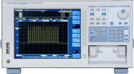
Yokogawa AQ6370 OPTICAL SPECTRUM ANALYZER. The AQ6370 uses a double-pass monochromator structure to achieve high wavelength resolution (0.02 nm) and wide close-in dynamic range (70 dB). Thus, closely allocated signals and noise can be separately

Used SMT Equipment | In-Circuit Testers
Yokogawa AQ6370 OPTICAL SPECTRUM ANALYZER. The AQ6370 uses a double-pass monochromator structure to achieve high wavelength resolution (0.02 nm) and wide close-in dynamic range (70 dB). Thus, closely allocated signals and noise can be separately

Used SMT Equipment | In-Circuit Testers
Yokogawa AQ6370 OPTICAL SPECTRUM ANALYZER. The AQ6370 uses a double-pass monochromator structure to achieve high wavelength resolution (0.02 nm) and wide close-in dynamic range (70 dB). Thus, closely allocated signals and noise can be separately
Technical Library | 2015-08-20 15:18:38.0
Increasing system integration and component densities continue to significantly reduce the opportunity to access nets using standard test points. Over time the size of test points has been drastically reduced (as small as 0.5 mm in diameter) but current product design parameters have created space and access limitations that remove even the option for these test points. Many high speed signal lines have now been restricted to inner layers only. Where surface traces are still available for access, bead probe technology is an option that reduces test point space requirements as well as their effects on high speed nets and distributes mechanical loading away from BGA footprints enabling test access and reducing the risk of mechanical defects associated with the concentration of ICT spring forces under BGA devices. Building on Celestica's previous work characterizing contact resistance associated with Pr-free compatible surface finishes and process chemistry; this paper will describe experimentation to define a robust process window for the implementation of bead probe and similar bump technology that is compatible with standard Pb-free assembly processes. Test Vehicle assembly process, test methods and "Design of Experiments" will be described. Bead Probe formation and deformation under use will also be presented along with selected results.


