Used SMT Equipment | In-Circuit Testers
Rohde & Schwarz ZNB8 Vector Network Analyzer, 2 Port, 8.5 GHz, N The R&S ZNB vector network analyzers feature a wide dynamic range of up to 140 dB (at 10 Hz IF bandwidth), low trace noise of less than 0.004 dB RMS (at 10 kHz IF bandwidth) and h
Industry Directory | Manufacturer
We specialize in Flex PCBs, Ridgid Flex, Long Flex PCBs and RF (radio frequency) Boards. Our engineering team has seen it all.
Industry Directory | Manufacturer
UWELLPCB.com is the PCB supplier. We offer PCB from single side board, double side PCB to 32layer board,including the Rigid PCB, Flex PCB, Rigid-flex PCB,Quick-turn prototype and PCB assembly

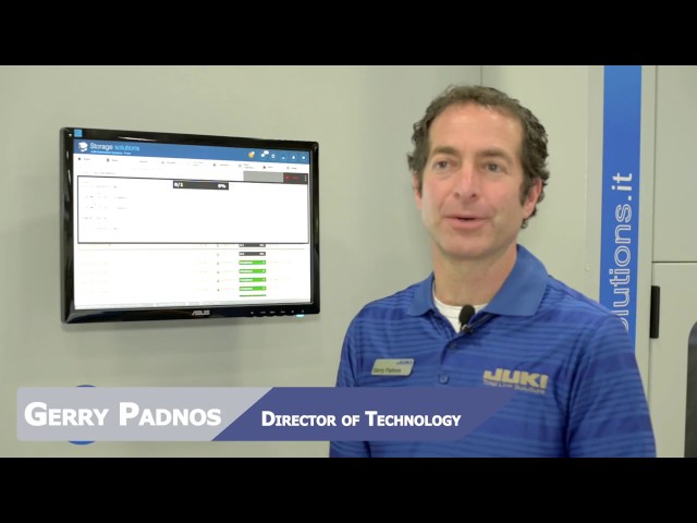
JUKI Automation Systems at the IPC Apex 2015; showcasing Intelligent Storage Systems.
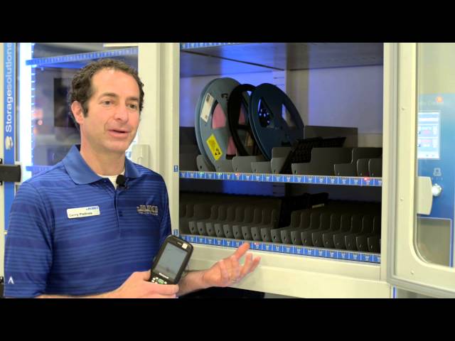
JUKI Automation Systems at the IPC Apex 2015; showcasing Intelligent Storage Systems.
Industry Directory | Consultant / Service Provider / Manufacturer
Tropical Stencil is dedicated to providing the highest quality Laser Cut Stencils; with our rapid response, you will have your Stencil delivered on-time.
Industry Directory | Manufacturer
Asia Pacific Circuits is one of Asia's leading Electronic Manufacturing Services companies, committed to providing high quality PCB and PCBA Contract Electronics Manufacturing Services.
Technical Library | 2020-09-02 22:02:13.0
With the adoption of Wafer Level Packages (WLP) in the latest generation mobile handsets, the Printed Circuit Board (PCB) industry has also seen the initial steps of High Density Interconnect (HDI) products migrating away from the current subtractive processes towards a more technically adept technique, based on an advanced modified Semi Additive Process (amSAP). This pattern plate process enables line and space features in the region of 20um to be produced, in combination with fully filled, laser formed microvias. However, in order to achieve these process demands, a step change in the performance of the chemical processes used for metallization of the microvia is essential. In the electroless Copper process, the critical activator step often risks cross contamination by the preceding chemistries. Such events can lead to uncontrolled buildup of Palladium rich residues on the panel surface, which can subsequently inhibit etching and lead to short circuits between the final traces. In addition, with more demands being placed on the microvia, the need for a high uniformity Copper layer has become paramount, unfortunately, as microvia shape is often far from ideal, the deposition or "throw" characteristics of the Copper bath itself are also of critical importance. This "high throwing power" is influential elsewhere in the amSAP technique, as it leads to a thinner surface Copper layer, which aids the etching process and enables the ultra-fine features being demanded by today's high end PCB applications. This paper discusses the performance of an electroless Copper plating process that has been developed to satisfy the needs of challenging amSAP applications. Through the use of a radical predip chemistry, the formation, build up and deposition of uncontrolled Pd residues arising from activator contamination has been virtually eradicated. With the adoption of a high throwing power Copper bath, sub 30um features are enabled and microvia coverage is shown to be greatly improved, even in complex via shapes which would otherwise suffer from uneven coverage and risk premature failure in service. Through a mixture of development and production data, this paper aims to highlight the benefits and robust performance of the new electroless Copper process for amSAP applications
JUKI Automation Systems at the IPC Apex 2015; showcasing Intelligent Storage Systems.


