

Plug into a DIP socket and provide a land pattern for soldering down an SOIC or SSOP device. Use to replace unavailable packages.
Career Center | Auckland, New Zealand | Engineering
NAVMAN PCBA NPI Engineer Reporting To: PCBA NPI Technical Leader Primary Objective: Transition of PCBs from R&D design to a manufacturable state conforming to all facets of PCBA production Secondary: Develop DFM & best practice guidelines Res
Industry News | 2002-03-27 08:18:37.0
SMT Plus and Accelerated Designs (ADI) have entered into a joint agreement to provide customers with CAD library software solutions. SMT Plus is a provider of land pattern libraries and training, while ADI performs PCB design and develops translator and library software.
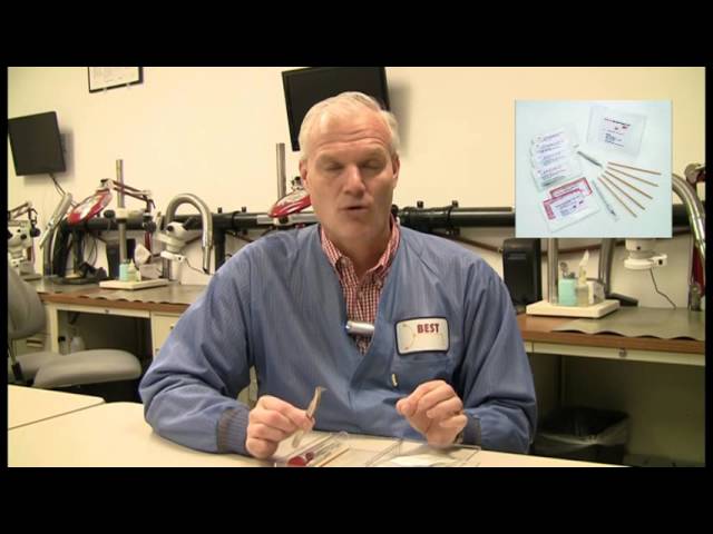
New Equipment | Rework & Repair Equipment
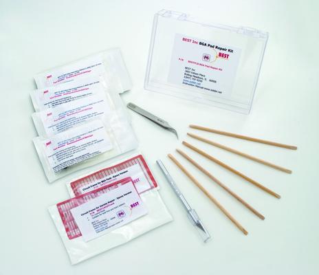
The BEST micro pad repair kit includes the tools and materials needed to reliably replace lifted or damaged surface mount and BGA pads on PCBs. This kit includes 3 different tin plated circuit frame patterns, which offer nearly 3 times as many useabl
New Equipment | Design Services
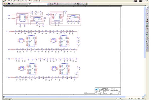
Even the best schematic circuit design can be undermined by poor component layout and routing. STI’s experienced design engineers address the critical design factors that affect manufacturing and assembly, product performance, and long-term reliabili
Industry News | 2009-07-15 16:25:41.0
MARIETTA, GA — July 2009 — PCB Matrix, a Valor Computerized Systems Ltd. company that focuses on EDA efficiency, productivity and automation, introduces the FREE Schematic Symbol Viewer, a cross platform correlation tool that allows users to import schematic symbols from multiple EDA formats and libraries, which is freely downloadable from the PCB Matrix Web site.
New Equipment | Rework & Repair Equipment
The BEST Pad Repair kit dry film version includes the tools and materials needed to reliably replace lifted or damaged surface mount and BGA pads on PCB's. This kit includes 3 different tin plated copper base material circuit frame patterns, which of
Career Center | Sherman, Texas USA | Engineering,Production,Research and Development,Technical Support
SMT Packaging Engineer: Location: Texas - Sherman , TX Group: HVAL Degree Requirements: BS ME/ChemE/Materials The person in this position will have the ability to make very significant financial contributions to TI because this is a very critic
New Equipment | Design Services
STI’s engineering team places emphasis on defect prevention and non-value added process step elimination by analyzing the design data package for common errors relating to the BOM selection, PCB design, and manufacturing materials/processes used to a
The BEST PCB pad repair repair kit gives you the tools you need for fast modification and repair of PCB circuit pads-no matter what their size. Our online PCB repair training videos, our master instructors along with these materials allows you to mee

PCB Libraries' "Footprint Expert" suite uses CAD LEAP(tm) Technology to greatly simplify footprint and 3D STEP model creation; it is used by tens of thousands of PCB designers and engineers all over the world.
Other / Media / Publisher / Online Resource / Consultant / Service Provider
24654 N. Lake Pleasant Pkwy
Peoria, AZ USA
Phone: 847-557-2300


