SOLDER PASTE STENCILS, LASER CUT,CHEM ETCH & ELECTROFORMED
Industry Directory | Manufacturer
Electroform, laser cut, and chem-etch stencils, precision chem-etch metal parts, inspection templates, mesh printing screens. IN BUSINESS OVER 30 YEARS!
New Equipment | Solder Paste Stencils
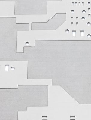
Laser cut stainless steel stencil with etched areas. When huge open spaces have to be produced on the bottom side of a stencil, the etching technology is one opportunity to realize it. The apertures for the solder paste print process are still manuf
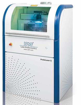
The next generation of in-house prototyping Laser-based PCB production can achieve much greater circuit detail, and lasers structure circuits significantly faster. This technology provides true on-demand production solution for both prototyping and
Electronics Forum | Tue Aug 04 18:23:19 EDT 1998 | john
We are looking for chem etching equipment. Does anyone know where I can find chem / laser systems?
Electronics Forum | Mon Jul 26 17:57:50 EDT 2021 | cyber_wolf
Place a label and etch that instead of the PCB. Too many variances in solder mask
Used SMT Equipment | Labeling Systems
Watch This Laser In action on YouTube Simplimatic Automation Cimtrak Laser Marker Model 3341. Fully Service and completely tested. 100% production ready. Contact for details, demo or video. Also have in stock matching Destaker, Flipper and Resta

Used SMT Equipment | Labeling Systems
Simplimatic Automation Cimtrak PCB Laser Etch / Marker System Like New Condition & video on YouTube Model: 3341 Date: 2014 200-240 VAC Single Phase 26A 2D Barcode ability Fully Automated Inline 36" Line Length Fully Ser
Industry News | 2003-03-21 08:12:24.0
Tecan reckons it is consistently producing what may be regarded as the most efficient stencils in the world today.
Industry News | 2012-02-28 19:55:52.0
Count On Tools has added a Laser Marking & Engraving capability to its manufacturing operations at its facility in Gainesville, GA. The recent expansion is in response to the growing market for SMT nozzles and consumables as well as the increased demand for its precision contract machining services.
Technical Library | 2024-09-03 16:33:11.0
The differences between chemical etching and laser milling are compared.
Technical Library | 2020-03-26 14:55:29.0
This paper introduces line confocal technology that was recently developed to characterize 3D features of various surface and material types at sub-micron resolution. It enables automatic microtopographic 3D imaging of challenging objects that are difficult or impossible to scan with traditional methods, such as machine vision or laser triangulation.Examples of well-suited applications for line confocal technology include glossy, mirror-like, transparent and multi-layered surfaces made of metals (connector pins, conductor traces, solder bumps etc.), polymers (adhesives, enclosures, coatings, etc.), ceramics (components, substrates, etc.) and glass (display panels, etc.). Line confocal sensors operate at high speed and can be used to scan fast-moving surfaces in real-time as well as stationary product samples in the laboratory. The operational principle of the line confocal method and its strengths and limitations are discussed.Three metrology applications for the technology in electronics product manufacturing are examined: 1. 3D imaging of etched PCBs for micro-etched copper surface roughness and cross-sectional profile and width of etched traces/pads. 2. Thickness, width and surface roughness measurement of conductive ink features and substrates in printed electronics applications. 3. 3D imaging of adhesive dots and lines for shape, dimensions and volume in PCB and product assembly applications.

For more information visit: http://www.lpkfusa.com/pls/ The LPKF ProtoLaser S is a fully enclosed laser system for PCB prototyping and production on-demand. It combines advanced laser technology, optics, and x/y table mechanisms that result in high
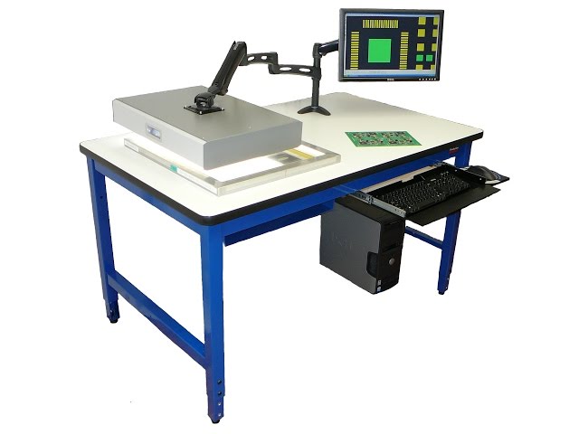
World's leading solder paste stencil & emulsion screen inspection system. Used by both stencil/screen fabricators and users to detect errors BEFORE production, eliminating costly rework, scrap and delays. Supports E-form, laser cut, chem etch, hybrid
Career Center | Ft Wayne, Indiana USA | Management,Production,Quality Control
Metal Etching Technology Inc. is one of the United States leading manufacturers of solder paste stencils for the electronics industry. Candidate's main responsibility will be to run a stencil laser cutting system for the printed circuit board indus
Career Center | Racine, Wisconsin USA | Engineering
Cree currently has a job vacancy for an SMT Process Technician in our Lighting Manufacturing facility in Racine, Wisconsin. Summary: This person will be a primary contributor to the startup of a new SMT production line for LED PCB Assembly. This
Blackfox Training Institute, LLC | https://www.blackfox.com/blackfox-how-to-make-a-printed-circuit-board-at-home/
. The materials you will need for making your own PCB are: magazines or advertising brochures laser printer or photocopier household clothes iron copper clad laminate etching solution kitchen scrubs thinner (acetone
| http://etasmt.com/cc?ID=te_news_industry,26765&url=_print
SMT Stencil step-by-step tutorial TYPES OF SMT STENCILS: Laser cut stencils are the most cost effective and the most commonly used in PCB assembly


winsouce.jpg)