
The PCB Footprint Expert is a powerful CAD library development tool powered by our own proprietary CAD LEAP Technology (Libraries Enhanced with Automated Preferences). It is packed with very powerful advanced library management features that cuts foo
New Equipment | Test Equipment
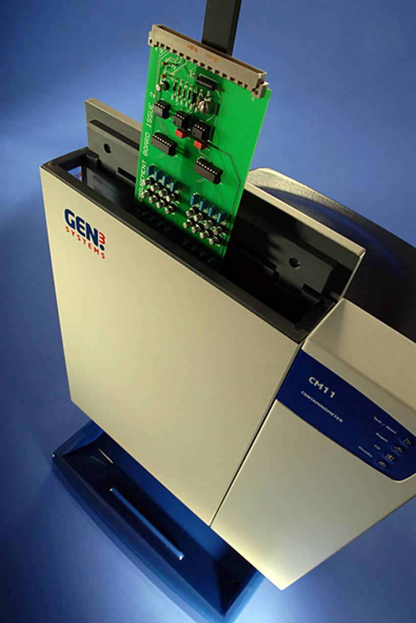
For over 40 years the Benchmark for Ionic Contamination Testing Commonly referred to "Cleanliness Testing" as this test method has, for over 40 years, been acknowledged as an important Quality Assurance and Process Control tool in the manufacture of
Electronics Forum | Wed Aug 23 11:06:57 EDT 2017 | cyber_wolf
Bad Z-force sensor or it is checking the board height in a hole.
Electronics Forum | Mon Aug 21 11:38:20 EDT 2017 | smdbert
Hello , How to solve this problem. Thnxs Bert
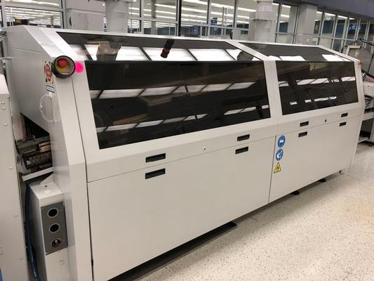
Used SMT Equipment | Soldering - Reflow
Vitronics 6622CC (Pb Free) Wave Soldering Machine Brand: Vitronics Model: 6622CC Vintage: 2001 Serial Number: 0103652201 LEADFREE unit Configured with Main Wave and Chip Wave Basic system according to General Specification (GS 235) CONTRO
Industry News | 2003-03-07 08:28:53.0
NPL now offers an on-site Lead-Free Health Check, where the issues brought to bear by lead-free are examined in the context of your company.
Industry News | 2010-10-01 00:32:52.0
MIRTEC, “The Global Leader in Inspection Technology”, announced that it will premier its complete line of inspection systems at in booth #7326 at the upcoming SMTA International, scheduled to take place October 26-27, 2010 at the Walt Disney World Swan and Dolphin Resort in Orlando, FL.

Parts & Supplies | Screen Printers
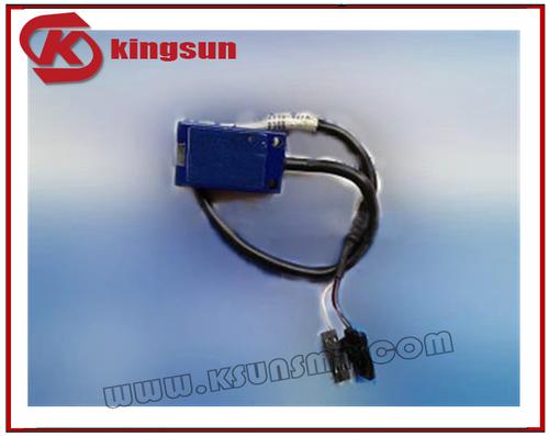
Product Name: CA-1115-02 SC300A-500FP sensor circuit breakers Part Number: CA-1115-02; SC300A-500FP Description: CA-1115-02; SC300A-500FP sensor circuit breakers Applicable models: AP Printing Presses CA-1115-02; SC300A-500FP circuit breake
Parts & Supplies | SMT Equipment
Sensor circuit breakers of MPM (CA-1115-02) Product Name: CA-1115-02 SC300A-500FP sensor circuit breakers Part Number: CA-1115-02; SC300A-500FP Description: CA-1115-02; SC300A-500FP sensor circuit breakers Applicable models: AP Printing Presses
Technical Library | 2017-12-11 22:31:06.0
Typical printed circuit board assemblies (PCBAs) processed by reflow, wave, or selective wave soldering were analysed for typical levels of process related residues, resulting from a specific or combination of soldering process. Typical solder flux residue distribution pattern, composition, and concentration are profiled and reported. Presence of localized flux residues were visualized using a commercial Residue RAT gel test and chemical structure was identified by FT-IR, while the concentration was measured using ion chromatography, and the electrical properties of the extracts were determined by measuring the leak current using a twin platinum electrode setup. Localized extraction of residue was carried out using a commercial C3 extraction system. Results clearly show that the amount and distribution of flux residues are a function of the soldering process, and the level can be reduced by an appropriate cleaning. Selective soldering process generates significantly higher levels of residues compared to the wave and reflow process. For conformal coated PCBAs, the contamination levels generated from the tested wave and selective soldering process are found to be enough to generate blisters under exposure to high humidity levels.
Technical Library | 2018-09-21 10:12:53.0
Moisture accumulates during storage and industry practice recommends specific levels of baking to avoid delamination. This paper will discuss the use of capacitance measurements to follow the absorption and desorption behaviour of moisture. The PCB design used in this work, focused on the issue of baking out moisture trapped between copper planes. The PCB was designed with different densities of plated through holes and drilled holes in external copper planes, with capacitance sensors located on the inner layers. For trapped volumes between copper planes, the distance between holes proved to be critical in affecting the desorption rate. For fully saturated PCBs, the desorption time at elevated temperatures was observed to be in the order of hundreds of hours. Finite difference diffusion modelling was carried out for moisture desorption behaviour for plated through holes and drilled holes in copper planes. A meshed copper plane was also modelled evaluating its effectiveness for assisting moisture removal and decreasing bake times. Results also showed, that in certain circumstances, regions of the PCB under copper planes initially increase in moisture during baking.
To see more visit Pillarhouse here: https://www.pillarhouse.co.uk/products/selective-soldering-handload/pilot-handload Economical, compact, single point selective soldering system The all-new ultra-low-cost Pilot machine has been designed as an ent

The PCB Footprint Expert is a powerful CAD library development tool powered by our own proprietary CAD LEAP Technology (Libraries Enhanced with Automated Preferences). It is packed with very powerful advanced library management features that cuts foo
Events Calendar | Mon Feb 19 00:00:00 EST 2024 - Mon Feb 19 00:00:00 EST 2024 | ,
SMTA Webinar: Development of Wireless Strain Measurement for Printed Circuit Board
Events Calendar | Mon Jun 08 00:00:00 EDT 2020 - Mon Jun 08 00:00:00 EDT 2020 | ,
Practical Set-Up, Qualification of Cleaning Process in PCB Assembly
Career Center | Orange County, California USA | Quality Control
Job Description: Summary: Reporting to the COO/CTO the VP of Quality role will involve creating and/or augmenting the Quality system and programs to be a pro-active vs. a reactive structure. This will involve creating an overall quality vision, se
Career Center | Chandler, Arizona USA | Technical Support
Koh Young America is looking for technical field application engineers to support our world class electronics 3D measurement and inspection products. This a dynamic position and will require skills to handle both technical pre-sales activities, s
Career Center | , India | Maintenance
Have worked in ELECTRONICS MANUFACTURING & SEMICONDUCTOR industry for 8+ years for machine maintenance worked with TDK CORPORATION (EPCOS PTE LTD) IN SINGAPORE FOR SEMICONDUCTOR worked with NOKIA INDIA PVT LTD IN INDIA FOR SMT MACHINE MAINTENANCE
Career Center | Melbourne, Florida USA | Management,Production,Quality Control
Technical Skills/Abilities: � Management � Quality Assurance � Strong Troubleshooting Skills � Strategic Planning � Employee Training � Quality Assurance � Problem Resolution � Mechanical/Technical Aptitude
PCB Libraries, Inc. | https://www.pcblibraries.com/forum/terminal-density-level-of-bga-footprints_topic3058_post12206.html
Terminal Density Level of BGA footprints - PCB Libraries Forum Forum Home > Libraries > Footprints / Land Patterns New Posts FAQ Search Events Register Login Terminal Density Level of BGA footprints
ASYMTEK Products | Nordson Electronics Solutions | https://www.nordson.com/en/divisions/march/about-us/events/wafer-level-packaging-symposium-2022
. One of these advanced technologies is silicon-based wafer-level packaging, such as fan-out wafer-level packaging. As the semiconductor industry shifts focus to more than

.gif)


winsouce.jpg)