GS Praezisions AG is a Swiss manufacturer of flex and rigid flex circuit boards. We spezialize in miniaturization and produce chip on board and flip chip substrates with micro via in laser and plasma technology among standard multilayer HDI PCBs.
Industry Directory | Manufacturer
We specialize in manufacturing high quality HDI PCBs.We manufactured lots of high complicated HDI PCBs(3+N+3,4+N+4,5+N+5,6+N+6,7+N+7 and micro-vias for anylayer) I will be happy to show some HDI PCBs we did if you have interest.
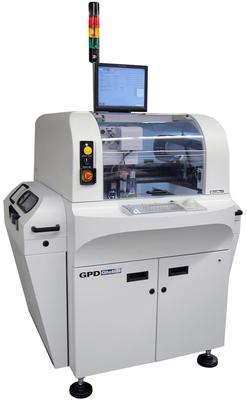
High Precision Dispensers - MAX Series (Non-Heated) Max Series is capable of a wide variety of dispense applications including MicroVolume, Solder Paste and Conductive Adhesive, Underfill, Surface Mount Adhesive, Dam and Fill, Encapsulations, LED En
New Equipment | Solder Paste Stencils
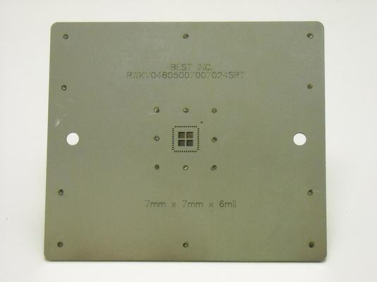
Based on its long work on BGA rework and repair process and its in-house capability to produce metal stencils BEST can provide for you a timely, cost-effective solution for printing on to components for MOST rework systems. Our templates for printing
Used SMT Equipment | Pick and Place/Feeders
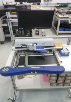
PROTOPLACE S - SEMI-AUTOMATIC SMT ASSEMBLY SYSTEM DESCRIPTION: SMT Pick & Place of PCB Prototypes The LPKF ProtoPlace S is an ergonomically designed, semi-automatic pick & place system for the professional assembly of SMT printed circuit board protot
Used SMT Equipment | In-Circuit Testers
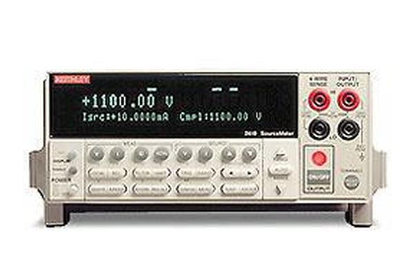
Keithley 2410 Model 2410 High-Voltage SourceMeter w/ Measurements up to 1100V and 1A, 20W Power Output Key Features and Benefits: New class of instruments designed for high speed DC testing Family of products offers wi
Industry News | 2011-09-12 12:04:25.0
GPD Global will showcase its Positive Cavity Displacement (PCD) 'H' Series high-resolution pumps in Booth #439 at the upcoming IMAPS 44th International Symposium on Microelectronics
Industry News | 2012-01-23 14:16:11.0
GPD Global will showcase its Positive Cavity Displacement (PCD) 'H' Series high-resolution pumps in Booth #2535 at the upcoming IPC APEX Expo.
Technical Library | 2001-04-24 10:44:24.0
This paper reviews the possible implementations of the Micro Via Technology within the Mentor Graphic's Board Station environment, specifically within the Librarian, Layout and Fablink applications. In this context, the definition of a Micro Via is constrained to Board Station’s support of such technology and contains only generalized descriptions of the manufacturing processes that require Micro Vias.
Technical Library | 2019-06-26 23:21:49.0
Copper-filled micro-vias are a key technology in high density interconnect (HDI) designs that have enabled increasing miniaturization and densification of printed circuit boards for the next generation of electronic products. Compared with standard plated through holes (PTHs) copper filled vias provide greater design flexibility, improved signal performance, and can potentially help reduce layer count, thus reducing cost. Considering these advantages, there are strong incentives to optimize the via filling process. This paper presents an innovative DC acid copper via fill formulation, for VCP (Vertical Continues Plating) applications which rapidly fills vias while minimizing surface plating.
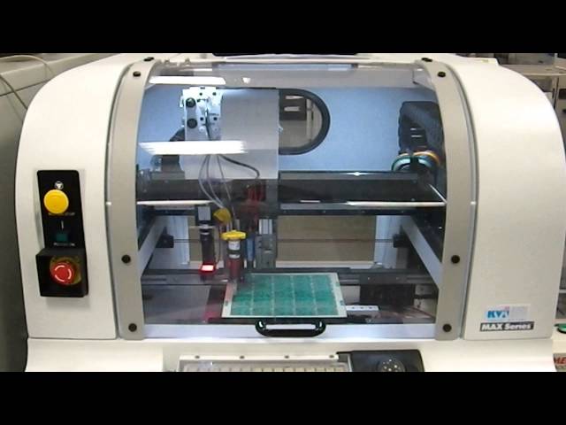
High Precision Dispensers - MAX Series (Non-Heated) Max Series is capable of a wide variety of dispense applications including MicroVolume, Solder Paste and Conductive Adhesive, Underfill, Surface Mount Adhesive, Dam and Fill, Encapsulations, LED En
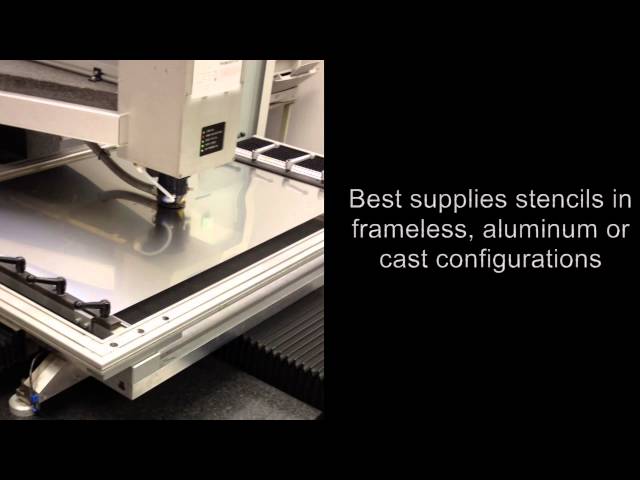
BEST manufactures and designs SMT stencils-both metal and plastic film type. This video demonstrates our metal stencil laser. See more on stencils here: http://www.soldertools.net/categories/Metal-Stencils/
Career Center | Columbia, Missouri USA | Engineering,Management,Production,Research and Development
I have a wide range of experience, from working for a defense contractor to one of the world’s largest manufacturers, with more recent experience in a start-up technology company. I have a Bachelor of Science Degree in Electrical Engineering from P
Career Center | San Jose, California USA | Engineering,Management,Research and Development
Ph.D., MBA, senior technical & management experience, advanced technology, electronics manufacturing processes, packaging, miniaturization, reliability, global team, PWB assembly, soldering Experience: 2001 - Flextronics, San Jose, CA Senior Manage
SMTnet Express, June 27, 2019, Subscribers: 32,092, Companies: 10,819, Users: 24,882 Advanced Cu Electroplating Process for Any Layer Via Fill Applications with Thin Surface Copper Credits: MacDermid Inc. Copper-filled micro-vias are a key
Imagineering, Inc. | https://www.pcbnet.com/capabilities/fabrication/hdi/
. Our micro via formation technology uses lasers to drill micro vias, also called blind via-holes (BVHs). With the ability to place on or off the pads, these holes let you selectively create routing room in denser parts of the substrate


