
Wafer-level Product In-line(Ireland) 2D, 3D CT AXI Machine Automatic inspection equipment exclusively for the Wafer-level products and ultra-fine defects of mm can be detected using the Nano Tube of Class Focal spot 200nm. 2D, as well as 70&o
Industry News | 2016-10-09 21:32:22.0
Topic: Study on a Formulated No Clean Flux for Fine-Pitch Flip Chip Package of Copper Pillar/ Micro-bump Interconnect. Time: October 18, 10:00 am – 1:30 pm Authors: Hsiang-Chuan Chen, Ya-Ching Chuang, Chia-Hao Chang, Watson Tseng
Industry News | 2020-12-24 05:12:18.0
X-ray inspection specialist, SEC Co., Ltd. is pleased to announce that since the launch of its industrial X-ray inspection equipment in October, the company has exceeded 1,500 units in cumulative sales volume. The company successfully developed the only industrial X-ray tube in Korea, and has maintained the No. 1 market share in Korea for many years based on the development of excellent systems suited to specific applications and competitive pricing.
Technical Library | 2015-12-02 18:32:50.0
(Thermal Compression with Non-Conductive Paste Underfill) Method.The companies writing this paper have jointly developed Copper (Cu) Pillar micro-bump and TCNCP(Thermal Compression with Non-Conductive Paste) technology over the last two+ years. The Cu Pillar micro-bump and TCNCP is one of the platform technologies, which is essentially required for 2.5D/3D chip stacking as well as cost effective SFF (small form factor) package enablement.Although the baseline packaging process methodology for a normal pad pitch (i.e. inline 50μm) within smaller chip size (i.e. 100 mm2) has been established and are in use for HVM production, there are several challenges to be addressed for further development for commercialization of finer bump pitch with larger die (i.e. ≤50μm tri-tier bond pad with the die larger than 400mm2).This paper will address the key challenges of each field, such as the Cu trace design on a substrate for robust micro-joint reliability, TCNCP technology, and substrate technology (i.e. structure, surface finish). Technical recommendations based on the lessons learned from a series of process experimentation will be provided, as well. Finally, this technology has been used for the successful launching of the company FPGA products with SFF packaging technology.
Technical Library | 2016-08-11 15:49:59.0
The challenge for 3D IC assembly is how to manage warpage and thin wafer handling in order to achieve a high assembly yield and to ensure that the final structure can pass the specified reliability requirements. Our test vehicles have micro-bumped die having pitches ranging from 60um down to 30um. The high density of pads and the large die size, make it extremely challenging to ensure that all of the micro-bump interconnects are attached to a thin Si-interposer. In addition, the low standoff between the die and interposer make it difficult to underfill. A likely approach is to first attach the die to the interposer and then the die/interposer sub-assembly to the substrate. In this scenario, the die/interposer sub-assembly is comparable to a monolithic silicon die that can be flip chip attached to the substrate. In this paper, we will discuss various assembly options and the challenges posed by each. In this investigation, we will propose the best method to do 2.5D assembly in an OSAT(Outsourced Assembly and Test) facility.
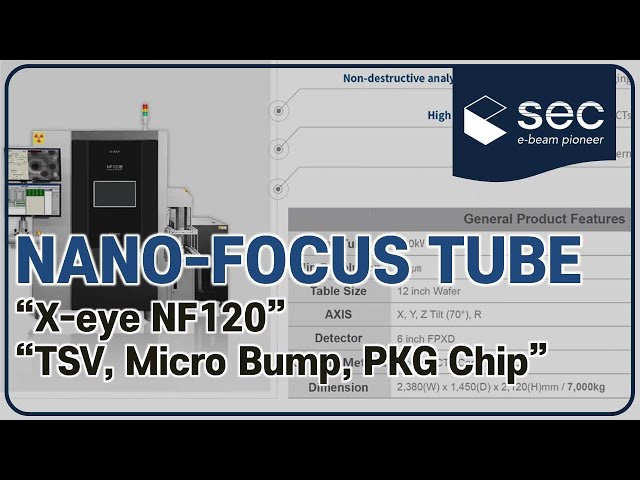
#Xray#Inspection#SEC Nano-focus Tube of 200 nano resolution which is specialized for sub-micron defects of Semiconductor Packaging, Wafer Level Packaging(WLP). -Non-destructive Analysis System -High-Resolution Image with Dual Type CTs -Application
HALT Testing of Backward Soldered BGAs on a Military Product Online Version SMTnet Express, December 10, 2015, Subscribers: 23,782, Members: Companies: 14,767, Users: 39,402 Packaging Technology and Design Challenge for Fine Pitch Micro-Bump Cu
HALT Testing of Backward Soldered BGAs on a Military Product Online Version SMTnet Express, December 10, 2015, Subscribers: 23,782, Members: Companies: 14,767, Users: 39,402 Packaging Technology and Design Challenge for Fine Pitch Micro-Bump Cu
Surface Mount Technology Association (SMTA) | https://www.smta.org/knowledge/proceedings_abstract.cfm?PROC_ID=4722
), the Ag3Sn precipitate morphology and on the mechanical properties of micro Cu pillar bumps were examined. The shear strength performance of micro Cu pillars with three different bump diameters (30µm, 50µm, and 100µm) was also evaluated


