
The RTI-7500, high-speed PCB inspection system, featuring high precision (1-micron accuracy), and color inspection option.
Micron, Motorola, NEC, Ohmron, Onsemi, Phillips, Texas Instruments and more.....
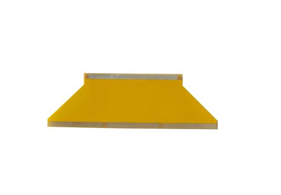
New Equipment | Solder Paste Stencils
MLT stainless steel and non-metal stencils (i.e. Kapton) are laser fabricated for applying solder paste, flux, solderballs, to circuit boards, wafers, and components for prototypes, volume production, and PCB rework.
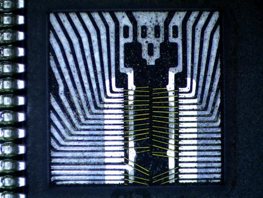
New Equipment | Rework & Repair Equipment
MLT provides laser decapsulation, "decap", services for removing encapsulation or mold compounds for accessing wirebonds, die, leadframes, and substrates.
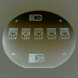
New Equipment | Fabrication Services
PFC designs, manufactures and assembles fine line flex circuits. 50 micon line and space is done in production on a daily basis. 37.5 microns done for prototoypes.
Technical Library | 2015-04-02 20:12:58.0
The demands on volume delivery and positioning accuracy for solder paste deposits are increasing as the size and complexity of circuits continue to develop in the electronics industry. According to the iNEMI 2013 placement accuracy for these kinds of components will reach 6 sigma placement accuracy in X and Y of 30 um by 2023.This study attempts to understand the dependencies on piezo actuation pulse profile on jetting deposit quality, especially focused on positioning, satellites and shape. The correlation of deposit diameter and positioning deviation as a function of piezo actuation profile shows that positioning error for deposits increase almost monotonically with decreasing droplet volume irrespective of the piezo-actuation profile. The trends for shape and satellite levels are not as clear and demand further study.
Technical Library | 2018-02-28 22:28:30.0
Circuit functional density requirements continue to drive innovative approaches to high performance packaging. Some new approaches include; aggressive space reduction, embedded solutions, and those that offer some form of risk reduction and rework potential are now options that are being explored by customers. Requirements for assembly of these types of packages necessitate the deposition of solder paste and assembly of components into cavities of the substrates to gain z-axis density as well as area functional density. Advances in the fabrication of PWB’s with cavities using newly developed laser micro-fabrication processes along with increased circuit pitch density of 50 micron lines and spaces permit new applications for high performance electronic substrates. First published at SMTA Pan Pacific Symposium
Technical Library | 2022-01-05 23:10:11.0
Waste electrical and electronic equipment or e-waste generation has been skyrocketing over the last decades. This poses waste management and value recovery challenges, especially in developing countries. Printed circuit boards (PCBs) are mainly employed in value recovery operations. Despite the high energy costs of generating crushed and milled particles of the order of several microns, those are employed in conventional hydrometallurgical techniques. Coarse PCB pieces (of order a few centimetres) based value recovery operations are not reported at the industrial scale as the complexities of the internal structure of PCBs limit efficient metal and non-metal separation.
Industry Directory | Distributor
We are independant stocking distributor of semiconductors, passive and relays, and electron tubes established since 1947. We are located in Belgium and serve OEM's, distributors and users worldwide.We are a product specialist meet
Welcome to the next generation in PWB test solutions. We combine an exceptional team of technology and applications experts with HIOKI's industry-leading systems to enhance your reliability and to speed up your product development process.

COT specializes in high quality SMT nozzles and consumables for pick and place machines. We provide special engineering design service of custom nozzles for those unique and odd components.
2481 Hilton Drive
Gainesville, GA USA
Phone: (770) 538-0411

.gif)
.gif)

