Industry Directory | Distributor
Custom-Fasteners.com specializes in manufacturing hard to find micro screws to specification, supplying OEMs and manufacturers worldwide.
Industry Directory | Distributor / Manufacturer
Design and manufacturing thick film printing machine for HIC,LTCC,HTCC,chip components,sensors,professional equipment provider,thick film printer,furnace, dryer,laser trimming,thick & thin film technology.

***V CUT PCB Depaneling machine*** 1. Easy maintenance and operation 2. Thin PCB even to 0.3mm can be sheared safely 3. Shearing process without vibrations due to pneumatic drive unit ***V CUT PCB depaneling machine specifications***

Details 1. Easy maintenance and operation 2. Thin PCB even to 0.3mm can be sheared safely 3. Shearing process without vibrations due to pneumatic drive unit Technical parameters Model CWVC-400 Max. PCB shearing length
Electronics Forum | Fri Sep 21 10:35:37 EDT 2012 | davef
Flash gold is just thin electrolytic gold plating over electroless nickel or electrolytic nickel. Flash gold plating ... * Less than 3 microinch thick will be porous and take solder poorly * Greater than 10 microinch thick will cause brittle solder c
Electronics Forum | Thu Sep 20 14:20:46 EDT 2012 | blnorman
From what I was told, gold flash normally refers to 10 microinches of gold.

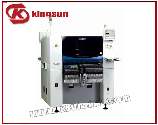
Used SMT Equipment | Pick and Place/Feeders
Product name: KE - 2060L JUKI chip mounter Product number: KE - 2060L JUKI2060 chip mounter parameters: Mounting head: 3 Material stand: 80 Mount speed: 0.25 SEC/CHIP (3 head at thesame time put in the attached SMT) Mounting speed:+ / - 0.. 5 M
Used SMT Equipment | Flexible Mounters
Product Name: Samsung high speed SM411 chip mounter Product number: SM411 Detailed product introduction Samsung high speed SM411 chip mounter parameters type: SM411 On the way: In - flight vision Number: 6 - axis *2 axis platform mount speed:
Industry News | 2003-05-19 10:06:43.0
The PCB is available with a maximum panel size of 406-by-460mm and a minimum board thickness of 0.8mm.
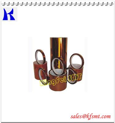
Parts & Supplies | Tape and Reel
SMT Kapton Tape Polymide film tape Specifications: Antistatic Thermally conductive Polyimides for fine line circuitry Cryogenic insulation Corona resistant Pigmented for color Conformable Other films tailored to meet customers needs Param
_1.jpg)
Parts & Supplies | Pick and Place/Feeders
N21005451AA PIN Other Panasonic parts: 1 KXFW1KWJA00 CLICK 1 3 N610033140AA OPERATING-SW 1 4 KXFA1PSTA01 COMB 1 5 KXFA1PSUA01 COMB 1 6 XSN25+3VW SCREW Cross recessed Pan head machine screw M2.5X3-A2-70 4 7 N210047118AB GEAR 2 8 KXFA1PS9A00 PI
Technical Library | 2021-07-20 20:02:29.0
During the manufacturing of printed circuit boards (PCBs) for a Flight Project, it was found that a European manufacturer was building its boards to a European standard that had no requirement for copper wrap on the vias. The amount of copper wrap that was measured on coupons from the panel containing the boards of interest was less than the amount specified in IPC-6012 Rev B, Class 3. To help determine the reliability and usability of the boards, three sets of tests and a simulation were run. The test results, along with results of simulation and destructive physical analysis, are presented in this paper. The first experiment involved subjecting coupons from the panels supplied by the European manufacturer to thermal cycling. After 17 000 cycles, the test was stopped with no failures. A second set of accelerated tests involved comparing the thermal fatigue life of test samples made from FR4 and polyimide with varying amounts of copper wrap. Again, the testing did not reveal any failures. The third test involved using interconnect stress test coupons with through-hole vias and blind vias that were subjected to elevated temperatures to accelerate fatigue failures. While there were failures, as expected, the failures were at barrel cracks. In addition to the experiments, this paper also discusses the results of finite-element analysis using simulation software that was used to model plated-through holes under thermal stress using a steady-state analysis, also showing the main failure mode was barrel cracking. The tests show that although copper wrap was sought as a better alternative to butt joints between barrel plating and copper foil layers, manufacturability remains challenging and attempts to meet the requirements often result in features that reduce the reliability of the boards. Experimental and simulation work discussed in this paper indicate that the standard requirements for copper wrap are not contributing to the overall board reliability, although it should be added that a design with a butt joint is going to be a higher risk than a reduced copper wrap design. The study further shows that procurement requirements for wrap plating thickness from Class 3 to Class 2 would pose little risk to reliability (minimum 5 μm/0.197 mil for all via types).Experimental results corroborated by modeling indicate that the stress maxima are internal to the barrels rather than at the wrap location. In fact, the existence of Cu wrap was determined to have no appreciable effect on reliability.
Technical Library | 2020-07-22 19:39:05.0
The PWB industry needs to complete reliability testing in order to define the minimum copper wrap plating thickness requirement for confirming the reliability of PTH structures. Predicting reliability must ensure that the failure mechanism is demonstrated as a wear-out failure mode because a plating wrap failure is unpredictable. The purpose of this study was to quantify the effects of various copper wrap plating thicknesses through IST testing followed by micro sectioning to determine the failure mechanism and identify the minimum copper wrap thickness required for a reliable PWB. Minimum copper wrap plating thickness has become an even a bigger concern since designers started designing HDI products with buried vias, microvias and through filled vias all in one design. PWBs go through multiple plating cycles requiring planarization after each plating cycle to keep the surface copper to a manageable thickness for etching. The companies started a project to study the relationship between Copper wrap plating thickness and via reliability. The project had two phases. This paper will present findings from both Phase 1 and Phase 2.

http://www.pcb-separator.com/plus/view.php?aid=86 PCB multi cutter machine/high efficiency PCB depaneling 900 machine/ PCB separator
http://www.pcb-separator.com/plus/view.php?aid=86 PCB multi cutter machine/high efficiency PCB depaneling 900 machine/ PCB separator
Training Courses | | | IPC J-STD-001 Trainer (CIT)
The Certified IPC J-STD-001 Trainer (CIT) courses prepare individuals as qualified trainers in the area of producing high quality soldered interconnections and prepares them to deliver Certified IPC J-STD-001 Specialist (CIS) training.
Training Courses | | | IPC-7711/7721 Trainer (CIT)
The Certified IPC-7711/7721 Trainer (CIT) courses recognize individuals as qualified trainers in the area of rework and repair of printed boards and electronic assemblies and prepares them to deliver Certified IPC-7711/7721 (CIS) training.
Events Calendar | Tue Jan 24 08:00:00 EST 2017 - Thu Jan 26 16:30:00 EST 2017 | Atlanta, Georgia USA
PLC Training Seminar
Career Center | Rolling Meadows, Illinois USA | Quality Control
Job: PCB Assembly/Soldering Instructor Responsibilities: Provide instruction to students in IPC classes IPC-A-610, IPC JSTD-001, IPC 7711/21, IPC-A-620 Provide instruction to students in BEST classes Provide course content for and instruction to stu
Career Center | Chesterland, Ohio USA | Production
Surface Grinder/Lapper Operator Position Overview We currently have an excellent career opportunity for a Surface Grinder/Lapper Operator to join our Ceramics team at our Channel Products, Inc. facility in Chesterland, OH. This position is respons
Career Center | Erode, Tamilnadu India | Engineering
Professional Summary 3+ years of experience in the PCB CAM engineering Exposure to FRONTLINE GENESIS 2000 Having exposure in UCAM Exposure to Create, Array & Panelize it for manufacturability Experienced in Creating impedance cou
Career Center | bangalore, India | Management
• Hands on experience in planning functions i.e. material planning, scheduling, inventory management. • We have a good knowledge of BOM, KANBAN, MIN-MAX order quantity, • We have Good knowledge in ERP Baan System , • Demand adjustment as per cu
PCB Libraries, Inc. | https://www.pcblibraries.com/Forum/ipc-class_topic2176_post9013.html
IPC Class - PCB Libraries Forum Forum Home > PCB Footprint Expert > Questions & Answers New Posts FAQ Search Events Register Login IPC Class Post Reply Author Message
| https://www.feedersupplier.com/sale-13118549-xp142-xp143-xp243-1mm-thickness-fuji-xp-smt-label-feeder.html
XP142 XP143 XP243 1mm Thickness Fuji XP SMT Label Feeder Basic Information Place of Origin: Japan Brand Name: FUJI Model Number: XP142/XP143/XP243 Minimum Order Quantity: 1 unit Price


